Choose Shipping Method
Shipping Method Estimated Delivery Time Shipping Cost
Home > Electronic Components, Accessories & Telecommunications > PCB & PCBA > Multilayer PCB > 48 hours for 6layer PCB quick ...
  • 0 Piece/Pieces $ 0
  • ship to United States To Be Negotiated $ /
  • Lead time / days
    After payment is complete, your order will ship within
  • Shipping time / days
    Estimated Delivery Time is the time between your package shipped out of carriers’ warehouses and final destination delivery. Estimated delivery time does not include supplier manufacturing lead time, holidays and weekends.
Totals $ /
48 hours for 6layer PCB quick turn
  • 48 hours for 6layer PCB quick turn
  • 48 hours for 6layer PCB quick turn
  • 48 hours for 6layer PCB quick turn
  • 48 hours for 6layer PCB quick turn
  • 48 hours for 6layer PCB quick turn
  • 48 hours for 6layer PCB quick turn
  • 48 hours for 6layer PCB quick turn
  • In Stock
  • Ready to Ship
  • Fast Dispatch

48 hours for 6layer PCB quick turn

  • $0.8
    ≥1
    Piece/Pieces
1 Piece/Pieces (Min. Order)
Quantity:

0 Piece,Product Price: US $ 0

  • Lead Time:/ days
  • Shipping time:/ days
Sample:
$5.00 /Piece/Pieces, 1 Piece/Pieces (Max. Order)Buy Samples
  • Product Description
Overview
Product Attributes
Model No.:
Quick turn PCB
place of origin:
China
Number of layers:
4-Layer, 6-Layer, 8-Layer, 10-Layer, 12-Layer
Min SMT Package:
0.201
Min IC pitch:
0.4mm
Max BGA size:
70*70mm
BGA ball pitch:
1.00 To 3.00mm
BGA ball diameter:
0.4 To 1.0mm
Surface Finishing::
Hal,Enig,Immersion Tin/Sliver
Testing Service::
Aoi X-Ray Function Test
Certificate::
Iso9001/Iatf16949/Iso13485
QFP lead pitch:
0.4 To 2.5mm
Packaging & Delivery
Selling Units:
Piece/Pieces
Single package size:
15cm*15cm*25cm
Single gross weight:
2kg
Package Type:
Vacuum and ESD Package
Picture Example:
Lead Time :
Quantity(Piece/Pieces) 1 ~ 2000>2000
Est. Time(days) 3To be negotiated

If you finish the payment today, your order will ship out within the delivery date.

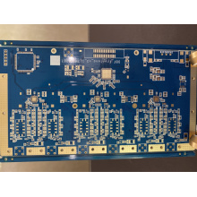
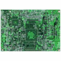
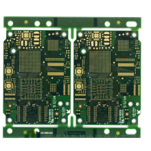
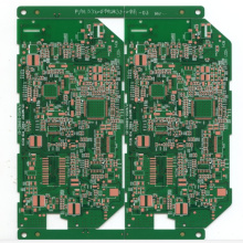
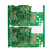
How is a 6 layer PCB made?

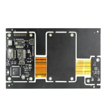
The 6-layer board can separate the analog ground from the digital ground because there can be two layers of ground in the PCB board. Regarding whether it is unified or separate, it involves the problem of the minimum return path of the signal in electromagnetic interference. After drawing the schematic diagram, don't forget to check the error and check the package manager to check the Electroniccomponents package. After the creation is completed, the schematic network table can be imported into the PCB file. The next thing to do is to set the layer structure (layer stack manager). add layer is to add an intermediate signal layer, and add plane is to add an internal power supply and an internal ground layer. The middle signal layer is the same as the top and bottom layers. Where signal lines are placed, the signal lines represent copper, and the places without signal lines are insulated. The internal power supply and the ground layer generate a copper mold. The line used when dividing the internal electrical layer represents the corroded copper, that is to say, the dark red represents the corroded copper, and the other areas represent the copper mold. Another point is that the power supply layer and the main ground layer should be tightly coupled, and an interval of 5 mils (prepreg) is preferable. The main principle of thebuile-up printed board layout is to do a good job of partitioning, that is, the partitioning of analog devices and digital devices, which can reduce interference, because the interference generated by digital signals is large, and the anti-interference is also strong, while the interference generated by analog signals is relatively small, but vulnerable Digital signal interference. Another point is to pay attention to the layout of components sourcing  with different operating voltages, and devices with large voltage differences should be far apart. For some Electronic Resistor and Capacitor decoupling capacitors, the closer to the pin, the better. The other thing to pay attention to is that the pins of the same network are close, and the communication PCB layout is beautiful.

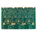
In principle, there are 3 signal layers and 3 power layers, of which GND is two layers 2, 5, and the middle layers 3 and 4 are Power and middle signal layers. If there are few wires in the middle signal layer,Metal Core PCB (MCPCB) copper can be applied to Power on the middle signal layer.

Each signal layer is adjacent to the inner electric layer, and there is no directly adjacent signal layer, which avoids signal crosstalk between layers;

The high-speed signal line can be arranged on the signal layer 5, so that it can be effectively shielded by the ground layer and the power layer. DRC inspection is very important. After the HDI  PCB board is drawn, it must be carried out to check whether there is anything that violates the rules and is not found.

48hours For 6layer Pcb 6 Jpg48hours For 6layer Pcb 5 Jpg48hours For 6layer Pcb 4 Jpg48hours For 6layer Pcb 3 Jpg48hours For 6layer Pcb 2 Jpg48hours For 6layer Pcb 1 Jpg

Wholesale 48 Hours For 6layer Pcb Quick Turn
Are you still worrying about not finding the 48 hours for 6layer pcb quick turn? Come and find the 48 hours for 6layer pcb quick turn you want on Bossgoomall. If you want to know more about the products in 48 hours for 6layer pcb quick turn, Please click on the product details to view. we have the perfect after-sales service and technical support. Looking forward to your use of our products.
Home > Electronic Components, Accessories & Telecommunications > PCB & PCBA > Multilayer PCB > 48 hours for 6layer PCB quick ...
Add To Cart Start Order
Sign in
Account
Password