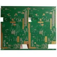
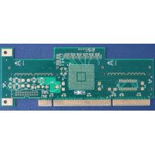
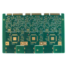
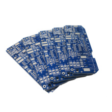
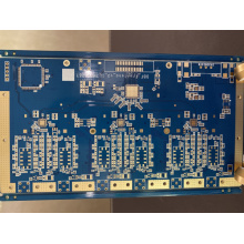
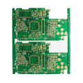
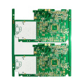
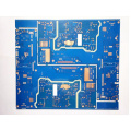
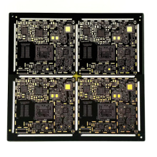
How is a PCB made step by step?
The process of Quickturn printed circuit board production is developing rapidly. Different types and different requirements of PCB adopt different processes, but the basic process flow is the same. Generally, it has to go through the processes of film plate making, pattern transfer, chemical etching, via and copper foil treatment, soldering and solder mask treatment.
The PCB manufacturing process can be roughly divided into the following four steps:
The first step of PCB production
1. Draw a base map
Most of the base maps are drawn by designers, and in order to ensure the High Quality Prototype PCB Fabrication of printed board processing, custom pcb fabrication needs to check and modify these base maps. If they do not meet the requirements, they need to be redrawn.
2. Photoengraving
Make a plate by taking a photo of the drawn base drawing of the board. The size of the layout should be consistent with the size of the PCB.
The process of PCB photographic plate making is roughly the same as that of ordinary photography, which can be divided into: film cutting-exposure-development-fixing-water washing-drying-revision. Before performing photography, check the correctness of the base map, especially the base map that has been placed for a long time.
Before exposure, the focal length should be adjusted, and the double-panel photographic plate should keep the same focal length of the front and back of the camera; after the photographic plate is dry, it needs to be revised.
The second step of PCB production graphics transfer
Transfer the PCB printed circuit pattern on the phase plate to the copper clad board, which is called PCB pattern transfer. There are many methods of PCB pattern transfer, and the commonly used methods are the silk screen printing method and the photochemical method.
1. Screen leakage
The screen leakage is similar to the mimeograph, which is to attach a layer of paint film or glue film on the screen, and then make the printed circuit diagram into a hollow pattern according to the technical requirements. The implementation of screen printing is an ancient printing process, simple to operate, Low Cost Prototype PCB; it can be realized by manual, semi-automatic or automatic screen printing machine. The steps for manual screen printing are as follows:
1) Position the copper clad board on the bottom plate, and put the printed material in the frame of the fixed screen.
2) Scrape the embossing material with a rubber plate, and make the screen and the copper clad laminate directly contact, then a composition pattern will be formed on the copper clad laminate.
3) Then dry and revise the version.
The third optical method of PCB production
(1) Direct photosensitive method
The process is as follows: surface treatment of the copper clad laminate, coating of photosensitive glue, exposure, development, solid film, and revision. Revision is the work that must be done before etching. Burrs, broken wires, sand holes, etc. can be repaired.
(2) Photosensitive dry film method
The process is the same as the direct photosensitive method, but instead of using photosensitive glue, a thin film is used as the photosensitive material. This kind of film is composed of three layers of materials: polyester film, photosensitive film and polyethylene film. The photosensitive film is sandwiched in the middle. The protective film of the outer layer is removed during use, and the photosensitive film is pasted on the copper-clad board using a film machine.
(3) Chemical etching
It uses chemical methods to remove unnecessary copper foil on the board, leaving behind the pads, printed wires and symbols that make up the pattern. Commonly used etching solutions include acid copper chloride, alkaline copper chloride, ferric chloride, etc.
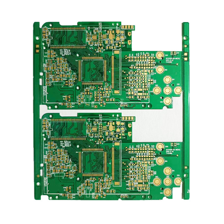
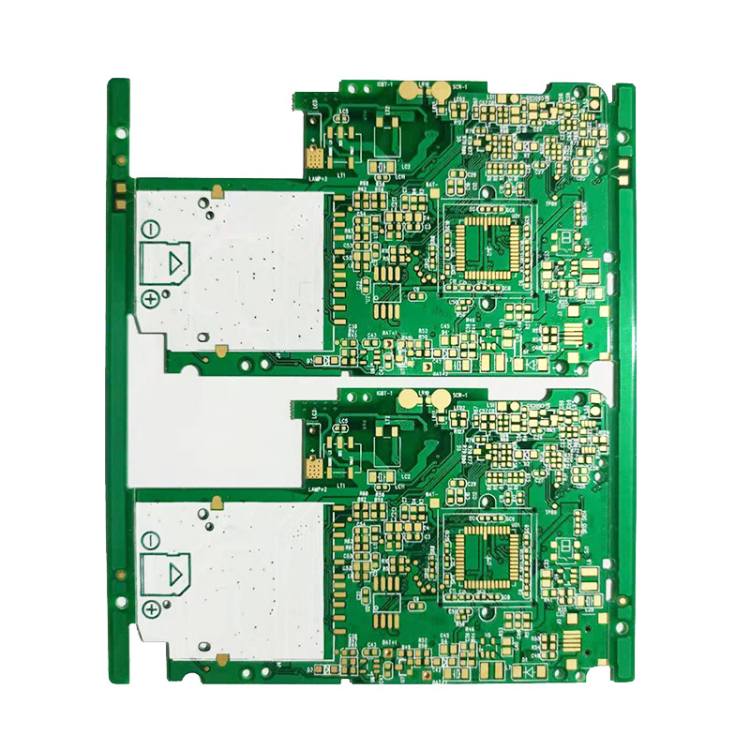
The fourth step of PCB production, via and copper foil processing
1. Metallized hole
The metallized hole is to deposit copper on the hole wall that penetrates the wires or pads on both sides, so that the original non-metallic hole wall is metalized, also called sinking copper. In double-sided and multilayer PCBs, this is an indispensable process.
The actual production has to go through a series of processes such as drilling, degreasing, roughening, immersion cleaning solution, hole wall activation, electroless copper plating, electroplating, and thickening.
The quality of the metallized holes is very important for double-sided PCBs, so they must be inspected. The metal layer is required to be uniform and complete, and the connection to the copper foil is reliable. In the surface-mounted high-density board, this kind of metallized hole adopts the blind hole method (the sinking copper fills the entire hole) to reduce the area occupied by the via hole and increase the density.
2. Metal coating
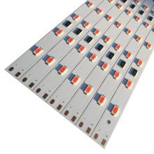
In order to improve the conductivity, solderability, wear resistance, and decoration of PCB printed circuits, extend the service life of the PCB, and improve electrical reliability, metal coating is often applied to the copper foil of the PCB. Commonly used coating materials include gold, silver and lead-tin alloys.
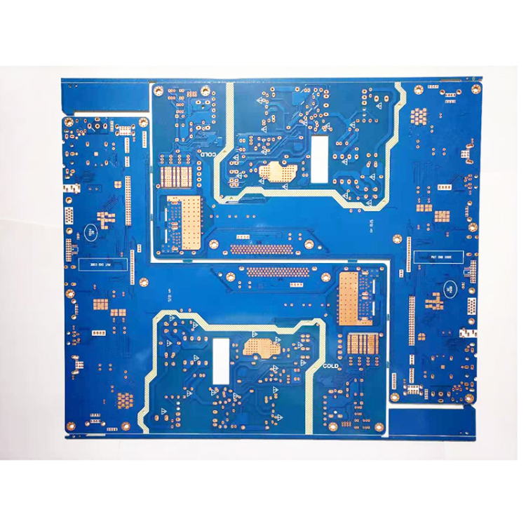
The fifth step of PCB production soldering assistance and solder mask treatment
After the PCB is coated with metal on the surface, it can be treated with flux or solder mask according to different needs. Applying flux can improve solderability; on high-density Metal Core PCB (MCPCB), in order to protect the board surface and ensure the accuracy of soldering, solder resist can be added to the board surface to expose the pads and other parts All under the solder mask. There are two types of solder resist coatings: heat curing type and light curing type. The color is dark green or light green.