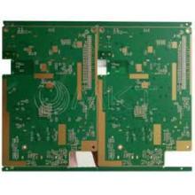
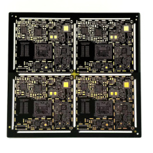
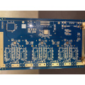
What is a 6-layer PCB?
Over the years, 0-18Layer FR4 board has gained great popularity in various industries. Nowadays, it is easy to find several types of multilayer PCB, including 4-layer PCB, 6-layer PCB, etc. The 6-layer PCB has become an integral part of compact wearable devices (Rigid-Flex Board) and other mission-critical communication devices. What makes them popular? How are they different from other types of multilayer PCBs?
Introduction to 6-layer PCB
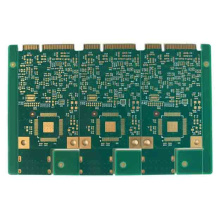
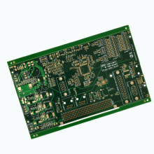
As the name implies, a six-layer PCB includes six layers of conductive materials. It is basically a 4-layer PCB with two additional signal layers placed between two planes. A typical 6-layer PCB stack has the following six layers: two inner layers, two outer layers, and two inner planes-one for power and the other for ground. This design improves EMI and provides better routing for low-speed and high-speed signals. Two surface layers help route low-speed signals, while two internal buried layers help route high-speed signals.
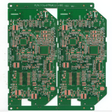
Shown above is a typical design of a 6-layer PCB; however, it may not be suitable for all applications. The next section will focus on some possible configurations of a 6-layer PCB.
Key factors to consider when designing 6-layer PCB stackups for different applications
The correct stacking of 6-layer PCB manufacturers can help you achieve better performance because it will help suppress EMI, use various types of RF equipment and include several fine-pitch PCB assemblies. Any errors in the stack-up design will seriously affect PCB performance. Where to start? This is how you correctly choose the stacking method.
As the first step of stacking design, it is important to analyze and solve the number of grounding, power and signal planes that the PCB may require.
Ground planes are an important part of any stackup because they provide better shielding for your PCB. Moreover, they minimize the need for external shielding tanks.
Here are some proven 6-layer PCB stackup designs for various applications:
For HDI PCBs with smaller footprints (HDI PCB): If you plan to route the dense boards with smaller footprints, you can install four signal planes, a ground plane and a power plane.
For denser circuit boards that will use a mixture of wireless/analog signals (Microwave radio frequency board): On this type of circuit board, you can choose a stack that looks like this: signal layer/ground/power layer/ground /Signal layer/Ground layer. In this type of stacking, the inner and outer signal layers are separated by two package ground layers. This laminated design helps to suppress EMI from mixing with the internal signal layer. The stack design is also ideal for RF equipment because the AC power supply and ground plane provide excellent decoupling.
For printed circuit boards with sensitive traces (high frequency mixing pressure plate): If you want to build a printed circuit board with many sensitive traces, it is best to choose a stack that looks like this: signal layer/power layer/ 2 signal layer/ground/signal layer. This stack will provide excellent protection for sensitive traces. The stack is suitable for circuits that use high-frequency analog signals or high-speed digital signals. These signals will be isolated from the low-speed signals on the outer layer. This shielding is done by the inner layer, which also allows the routing of signals with different frequencies or different switching speeds.
For boards that will be deployed near strong radiation sources: For this type of board, the stack of ground/signal layer/power/ground/signal layer/ground will be perfect. This stacking can effectively suppress EMI. This stack is also suitable for circuit boards used in noisy environments.
Benefits of using 6-layer PCB
Because of the six-layer PCB design, they have become a regular function in several advanced electronic circuits. The following advantages provided by these circuit boards make them very popular among electronics manufacturers.
Small footprint: Due to their multi-layer design, these printed circuit boards are smaller than other circuit boards. This is particularly beneficial for micro devices.
Quality-driven design: As mentioned earlier, 6-layer PCB stack-up design requires a lot of planning. This helps to reduce errors in details, thereby ensuring high-quality construction. In addition, nowadays, all major PCB manufacturers are adopting various testing and inspection techniques to ensure the suitability of these circuit boards.
Lightweight structure: A compact PCB is realized by using lightweight components, which helps reduce the overall weight of the PCB. Unlike single-layer or double-layer PCBs, six-layer circuit boards do not require multiple Electronic connectors to interconnect components.
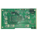
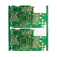
Improved durability: As shown in the figure above, these PCBs use multiple insulating layers between the circuits, and these layers are bonded with protective materials and different prepreg adhesives. This helps to improve the durability of these PCBs.
Excellent electrical performance: These printed circuit boards have excellent electrical performance to ensure high speed and high capacity in a compact design.