-
All Categories
- Agriculture
- Apparel
- Beauty & Personal Care
- Baby Care
- Bath Supplies
- Beauty Equipment
- Body Art
- Breast Care
- False Eyelashes & Tools
- Feminine Hygiene
- Fragrance & Deodorant
- Hair Care & Styling
- Hair Extensions & Wigs
- Makeup
- Makeup Tools
- Maternity Care
- Men's Grooming
- Nail Supplies
- Oral Hygiene
- Personal Hygiene Products
- Sanitary Paper
- Shaving & Hair Removal
- Skin Care
- Skin Care Tool
- Construction & Real Estate
- Balustrades & Handrails
- Bathroom & Kitchen
- Building Boards
- Building Glass
- Ceilings
- Corner Guards
- Countertops,Vanity Tops & Table Tops
- Curtain Walls & Accessories
- Decorative Films
- Door, Window & Accessories
- Earthwork Products
- Elevators & Escalators
- Fireplaces,Stoves
- Fireproofing Materials
- Floor Heating Systems & Parts
- Flooring & Accessories
- Formwork
- Heat Insulation Materials
- HVAC Systems & Parts
- Ladders & Scaffoldings
- Masonry Materials
- Metal Building Materials
- Mosaics
- Mouldings
- Multifunctional Materials
- Plastic Building Materials
- Real Estate
- Soundproofing Materials
- Stairs & Stair Parts
- Stone
- Tiles & Accessories
- Timber
- Wallpapers/Wall Coating
- Waterproofing Materials
- Consumer Electronics
- Blockchain Miners
- Camera, Photo & Accessories
- Chargers,Batteries & Power Supplies
- Commonly Used Accessories & Parts
- Computer Hardware & Software
- Earphone & Headphone
- Electronic Cigarettes
- Electronic Publications
- Home Audio, Video & Accessories
- Mobile Phone & Accessories
- Mobile Phone Parts
- Other Consumer Electronics
- Portable Audio, Video & Accessories
- Presentation Equipment
- Smart Electronics
- Speakers & Accessories
- TV Receivers & Accessories
- Video Games & Accessories
- Electrical Equipment & Supplies
- Electronic Components, Accessories & Telecommunications
- Acoustic Components
- Amplifiers and Comparators
- Capacitors
- Connectors and Accessories
- Crystals, Oscillators and Resonators
- Development Systems
- Diodes, Transistors and Thyristors
- Displays, Signage and Optoelectronics
- EL Products
- Electronic Accessories & Supplies
- Electronic Data Systems
- Electronic Signs
- Electronics Stocks
- Filters
- Inductors
- Integrated Circuits
- Optoelectronic Displays
- Optoelectronics
- Other Electronic Components
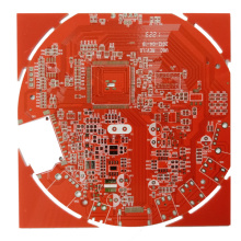
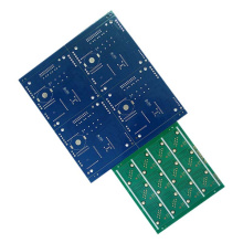
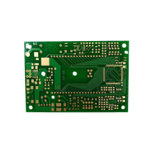
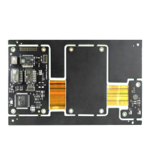
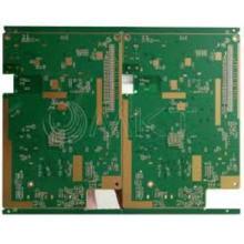
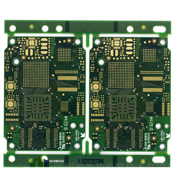
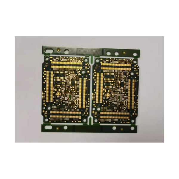
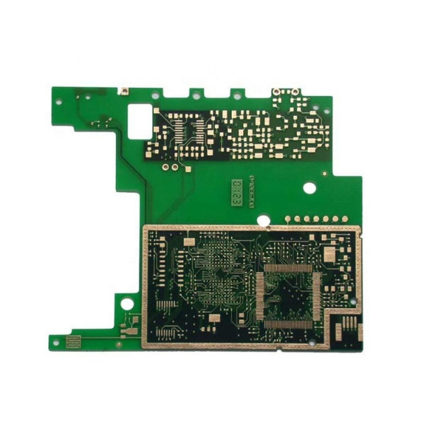
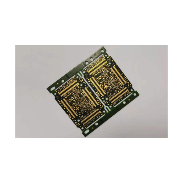
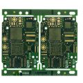
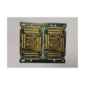
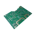
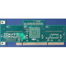
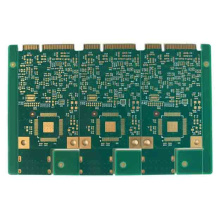
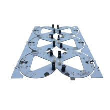
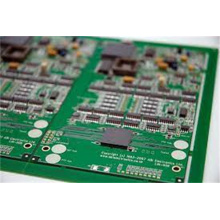
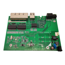
- PCB & PCBA
- Power Driver Modules
- Power Supplies and Circuit Protection
- Relay
- Resistors
- Sensors
- Switches
- Telecommunications
- Wireless & IoT
- Energy
- Environment
- Fabric & Textile Raw Material
- Fabrication Services
- Fashion Accessories
- More Categories
- Christmas Decoration Supplies
- Wedding Decoration & Supplies
- Kitchen Tools & Gadgets
- Bathroom Products
- Pet Products