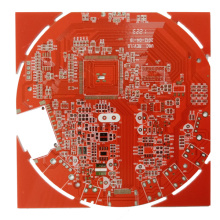
What is any layer PCB?
In recent years, in order to meet the miniaturization needs of some high-end consumer electronics products, the integration of origin electronics ICs has become higher and higher, the BGA pin pitch has become closer (less than or equal to 0.4 pitch), and the PCB layout has become more and more compact. , The trace density is also getting larger and larger. In order to improve the layout rate of the design without affecting the signal integrity and other performance, the ANYLAYER (any order) technology was born. This is the arbitrary via technology (ALIVH-Any Layer IVH Structure Multilayer). Printed Wiring Board).
Technical characteristics of any layer via
Comparing the characteristics of any layer via technology with HDI technology, the advantage of ALIVH is that the design freedom is greatly increased, and holes can be punched between layers at will, which cannot be achieved by HDI technology. Generally, domestic manufacturers achieve complex structures, that is, the design limit of HDI is a third-order HDI board. Since HDI does not completely use laser drilling, the buried holes in the inner layer use mechanical holes, so the requirement of the orifice disk is larger than that of the laser hole. There are many, and the mechanical hole takes up space on the level that it passes through. Therefore, in general, HDI structure has a big gap compared with the arbitrary perforation of ALIVH technology, and the inner core plate can also use 0.2mm micropores. Therefore, the wiring space of the ALIVH board is probably greatly improved than that of HDI. At the same time, the cost and processing difficulty of ALIVH is also higher than that of HDI process.
Design challenges of vias in any layer
Any layer via technology completely subverts the traditional via design method. If different layers of vias still need to be provided, it will increase the management difficulty. The design tool needs to have the ability of intelligent punching, and at the same time can be combined and split at will.
Cadence adds a working layer-based wiring method to the traditional wiring method based on the wiring layer, as shown in Figure 4: You can check the layer that can be looped in the Working Layer panel, and then double-click to punch , You can choose to switch lines between any layers.
Wiring method based on Working Layer
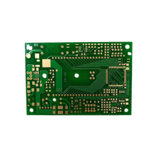
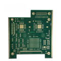
ALIVH design board example:
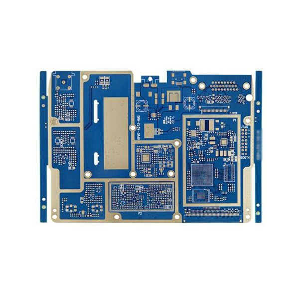
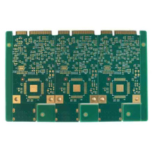
10-layer ELIC design
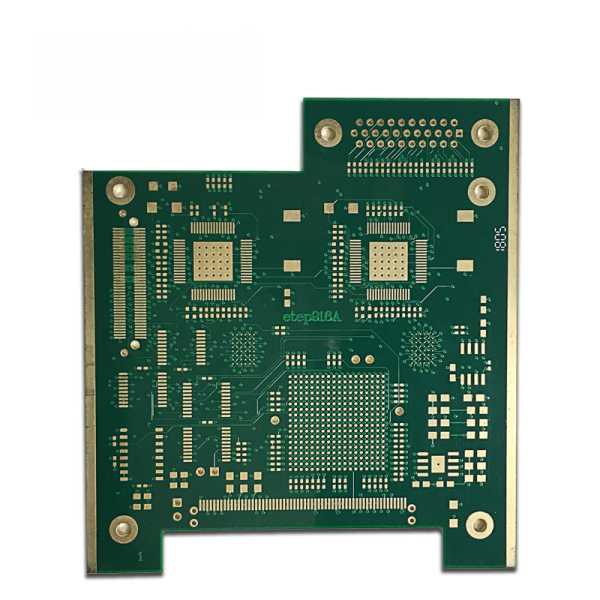
OMAP4 Platform
Buried Resistance, Buried Capacitance and Buried Electronic Components
High-speed access to the Internet and social networks requires high integration and miniaturization of handheld devices. Currently relying on 4-N-4 HDI technology. However, in order to achieve higher interconnection density in the next generation of new technologies, in this field, embedding passive or even active parts into PCBs and substrates can meet the above requirements. When you are designing consumer electronic products such as mobile phones and digital cameras, it is the current design choice to consider how to embed passive and active parts into the PCB and substrate. This method may be slightly different because you use different vendors. Another advantage of embedding parts is that the technology provides protection of intellectual property rights and prevents so-called reverse design. Allegro PCB Editor can provide industrial-grade solutions. Allegro PCB Editor can also work more closely with HDI PCB, Rigid-Flex Board and embedded parts. You can get the correct parameters and constraints to complete the design of embedded parts. The design of the embedded device can not only simplify the subsequent Surface-Mount (SMT) & BGA Assembly process, but also greatly improve the cleanliness of the product.
Buried resistance, buried capacitance design
Buried resistance, also known as buried resistance or thin film resistance, is to press a special resistance material on an insulating substrate, and then through printing, etching and other processes to obtain the required resistance value, and then press together with other PCB layers to form a plane Resistance layer. Common PTFE buried resistor multilayer printed board manufacturing technology can achieve the required resistance.
Buried capacitors use materials with higher capacitance density and reduce the distance between layers to form a large enough inter-plate capacitance to play the role of decoupling and filtering of the power supply system, thereby reducing the need for PCB Discrete capacitors, and can achieve better high-frequency filtering characteristics. Because the parasitic inductance of the embedded capacitor is very small, its resonant frequency point will be better than ordinary capacitors or low ESL capacitors.