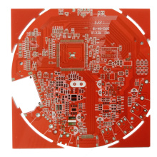
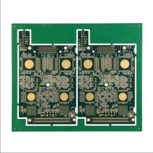
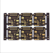
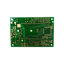
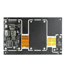
Choose Shipping Method
Shipping Method Estimated Delivery Time Shipping Cost
Home > Electronic Components, Accessories & Telecommunications > PCB & PCBA > Multilayer PCB > 16 Layerm Hdi Pcb Assembly Pcb...
  • 0 Piece/Pieces $ 0
  • ship to United States To Be Negotiated $ /
  • Lead time / days
    After payment is complete, your order will ship within
  • Shipping time / days
    Estimated Delivery Time is the time between your package shipped out of carriers’ warehouses and final destination delivery. Estimated delivery time does not include supplier manufacturing lead time, holidays and weekends.
Totals $ /
16 Layerm Hdi Pcb Assembly Pcba
  • 16 Layerm Hdi Pcb Assembly Pcba
  • 16 Layerm Hdi Pcb Assembly Pcba
  • 16 Layerm Hdi Pcb Assembly Pcba
  • 16 Layerm Hdi Pcb Assembly Pcba
  • 16 Layerm Hdi Pcb Assembly Pcba
  • 16 Layerm Hdi Pcb Assembly Pcba
  • 16 Layerm Hdi Pcb Assembly Pcba
  • In Stock
  • Ready to Ship
  • Fast Dispatch

16 Layerm Hdi Pcb Assembly Pcba

  • $120
    ≥1
    Piece/Pieces
1 Piece/Pieces (Min. Order)
Quantity:

0 Piece,Product Price: US $ 0

  • Lead Time:/ days
  • Shipping time:/ days
Sample:
$120.00 /Piece/Pieces, 1 Piece/Pieces (Max. Order)Buy Samples
  • Product Description
Overview
Product Attributes
Model No.:
HDI PCB Products
Number of layers:
4-Layer, 6-Layer, 8-Layer, 10-Layer, 12-Layer, 1-48
Base Material:
Fr4, High Tg Fr4, High Frequency, Alum, Fpc
Min. Hole Size:
0.2mm
Min. Line Width:
0.075mm
Min. Line Spacing:
0.075mm
Board Thickness:
0.1-4mm±10%, 0.1-4mm±10%
Copper Thickness:
0.5-4 0z
FOB Reference Price:
12
Get Latest Price:
Message Communication
Min line/space:
0.075/0.075mm
Packaging & Delivery
Selling Units:
Piece/Pieces
Single package size:
13cm*8cm*0.2cm
Single gross weight:
0.02kg
Picture Example:
Lead Time :
Quantity(Piece/Pieces) 1>1
Est. Time(days) 7To be negotiated

If you finish the payment today, your order will ship out within the delivery date.

What is HDI layout?

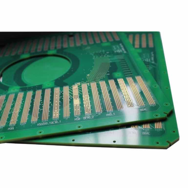
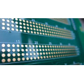
For HDI PCBs, apart from component and wiring density, almost nothing can distinguish these products from standard PCBs. I have seen designers point out that HDI boards refer to anything with 10 million or smaller vias, 6 million or smaller traces, or with 0.5 mm or smaller pin pitch. Your low cost 4 layer pcb supplier will tell you that HDI PCB uses blind holes about 8 mils or smaller, and the smaller blind holes are BVH PCBs drilled by laser.
In some respects, they are all correct, because there is no specific threshold for the composition of the HDI PCB layout. Everyone can agree that once the design includes microwells, it is an HDI board. In terms of design, you need to set certain design rules before you can touch the layout. Before establishing design rules, you should collect the capabilities of the manufacturer. After this is done, you need to set up design rules and some layout features
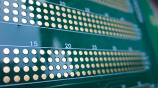
Trace width and via size. The width of a trace and its impedance and trace width will determine when you enter the HDI system. Once the trace width becomes small enough, the via will also become so small that it must be manufactured as a micro via.
Layer transition. The through hole needs to be carefully designed according to the aspect ratio, which also depends on the required layer thickness. Layer transitions should be defined early so that they can be placed quickly during the routing process.
gap. The traces must be separated from each other and kept separate from other objects (pads, components, planes, etc.) that are not part of the network. The goal here is to ensure compliance with HDI DFM rules and prevent excessive crosstalk.
Other trace restrictions, such as trace length adjustment, maximum trace length, and allowable impedance deviation during the trace process are also important, but they will apply to places other than HDI boards. Here, the two most important points are the via size and trace width. The gap can be determined in a variety of ways (for example, simulation) or following standard rules of thumb. Be careful with the latter, as this may result in excessive internal layer crosstalk or insufficient wiring density.

One Stop Bom Purchase Solution JpgLow Cost Prototype Pcb JpgFast Pcb Manufacture Low Cost JpgOnline Pcb Instant Quote JpgMetal Core Pcb Mcpcb Jpg1 8layer Fast Pcb Fabrication Jpg


Wholesale 16 Layerm Hdi Pcb Assembly Pcba
Are you still worrying about not finding the 16 layerm hdi pcb assembly pcba? Come and find the 16 layerm hdi pcb assembly pcba you want on Bossgoomall. If you want to know more about the products in 16 layerm hdi pcb assembly pcba, Please click on the product details to view. we have the perfect after-sales service and technical support. Looking forward to your use of our products.
Home > Electronic Components, Accessories & Telecommunications > PCB & PCBA > Multilayer PCB > 16 Layerm Hdi Pcb Assembly Pcb...
Add To Cart Start Order
Sign in
Account
Password