Choose Shipping Method
Shipping Method Estimated Delivery Time Shipping Cost
Home > Electronic Components, Accessories & Telecommunications > PCB & PCBA > Double-Sided PCB > Smart Bms Hdi Buried Blind PCB...
  • 0 Piece/Pieces $ 0
  • ship to United States To Be Negotiated $ /
  • Lead time / days
    After payment is complete, your order will ship within
  • Shipping time / days
    Estimated Delivery Time is the time between your package shipped out of carriers’ warehouses and final destination delivery. Estimated delivery time does not include supplier manufacturing lead time, holidays and weekends.
Totals $ /
Smart Bms Hdi Buried Blind PCB Powerbank PCBA
  • Smart Bms Hdi Buried Blind PCB Powerbank PCBA
  • Smart Bms Hdi Buried Blind PCB Powerbank PCBA
  • Smart Bms Hdi Buried Blind PCB Powerbank PCBA
  • Smart Bms Hdi Buried Blind PCB Powerbank PCBA
  • In Stock
  • Ready to Ship
  • Fast Dispatch

Smart Bms Hdi Buried Blind PCB Powerbank PCBA

  • $0.99
    ≥1
    Piece/Pieces
1 Piece/Pieces (Min. Order)
Quantity:

0 Piece,Product Price: US $ 0

  • Lead Time:/ days
  • Shipping time:/ days
  • Product Description
Overview
Product Attributes
Model No.:
Powerbank PCB PCBA
Base Material:
Fr4,
Min. Line Width:
0.075mm
Board Thickness:
0.1-4mm±10%, 0.1-4mm±10%
Min. Line Spacing:
0.075mm
Copper Thickness:
0.5-4 0z
Min. Hole Size:
0.2mm
Packaging & Delivery
Selling Units:
Piece/Pieces
Single package size:
12cm*8cm*0.02cm
Single gross weight:
0.036kg
Package Type:
Vacuum packing
Lead Time :
Quantity(Piece/Pieces) 1 ~ 1000>1000
Est. Time(days) 9To be negotiated

If you finish the payment today, your order will ship out within the delivery date.

What does PCB assembly mean?
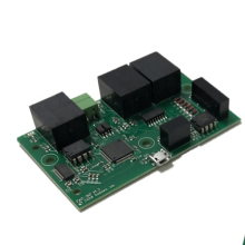
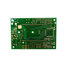
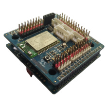
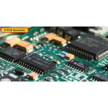
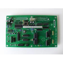
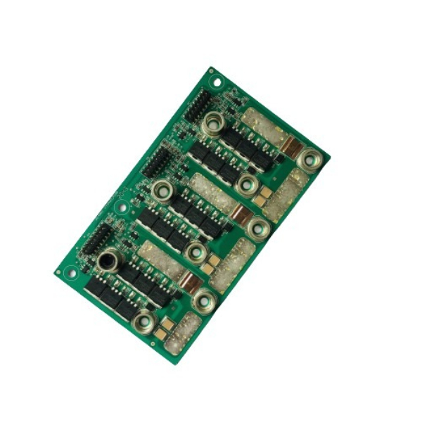
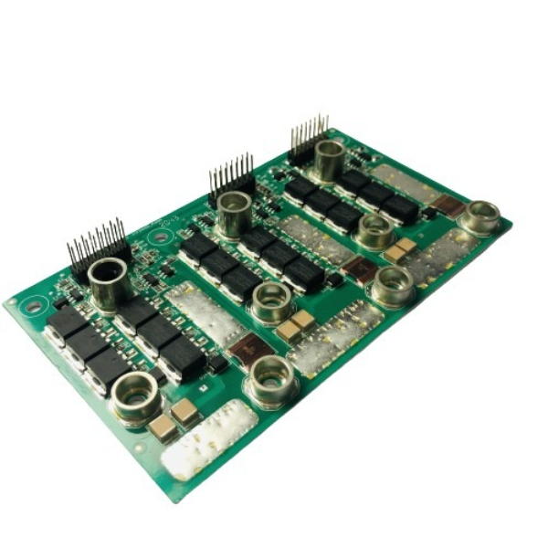
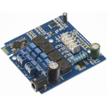
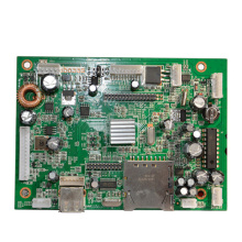
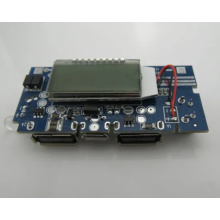
The assembly or manufacturing process of a printed circuit board (PCB) includes many steps. All these steps should go hand in hand to achieve good PCB assembly (PCBA). The synergy between one step and the previous step is very important. What steps are involved in the PCB assembly process?
Step 1: Add solder paste: This is the initial stage of the assembly process. At this stage, solder paste is added to the electronic components pads wherever soldering is required. Put the solder paste on the pad and paste it in the correct position with the help of the soldering screen. This screen is made of PCB files and has holes.
Step 2: Place components: Perform Surface-Mount (SMT) &BGA Assembly.
Step 3: Reflow oven: This step is used to permanently fix the components on the board. After placing the components on the board, the PCB passes through the reflow oven conveyor belt. The controlled heat of the oven melts the solder added in the first step, thereby permanently connecting the components.
Step 4: Wave soldering: In this step, the PCB is passed through a wave of molten solder. This will establish electrical connections between the solder, PCB pads and component leads.
Step 5: Cleaning: Up to this step, all soldering processes of Wave Solder for PCBA have been completed. During the soldering process, a large amount of flux residue will form around the solder joints. As the name suggests, this step involves cleaning flux residues. Clean the flux residue with deionized water and solvent. Through this step, PCB Mixed Assembly is completed. The next steps will ensure that the assembly is completed correctly.
Step 6: Testing: At this stage, the PCB Mixed Assembly is completed, and inspections are started to test the location of the components. This can be performed in two ways:
1. Manual: This kind of inspection is usually carried out for smaller components, and the number of components does not exceed one hundred.
2. Automatic: Perform this check to check whether there are bad joints, wrong components, wrongly placed components, etc.
Smart Bms Powerbank Pcba JpgSmart Bms Hdi Pcb JpgPowerbank Pcb Pcba Jpg
 

Wholesale Smart Bms Hdi Buried Blind Pcb Powerbank Pcba
Are you still worrying about not finding the smart bms hdi buried blind pcb powerbank pcba? Come and find the smart bms hdi buried blind pcb powerbank pcba you want on Bossgoomall. If you want to know more about the products in smart bms hdi buried blind pcb powerbank pcba, Please click on the product details to view. we have the perfect after-sales service and technical support. Looking forward to your use of our products.
Home > Electronic Components, Accessories & Telecommunications > PCB & PCBA > Double-Sided PCB > Smart Bms Hdi Buried Blind PCB...
Add To Cart Start Order
Sign in
Account
Password