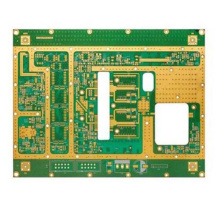
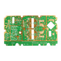
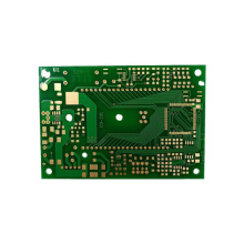
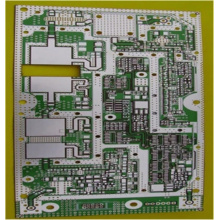
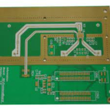
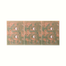
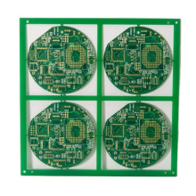
What is a multilayer PCB?
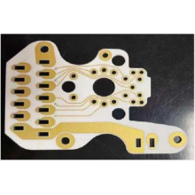
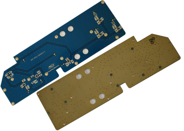
As the name suggests, a multi-layer board is composed of multiple single-sided boards. The introduction in professional books is: Stacked by three or more double panels. The use of multiple wire layouts significantly increases the area available for wiring. Usually, they are even-numbered layers. This is because in the PCBA Manufacturing process, odd-numbered layers can cause problems such as warpage and distortion.
1. Suitable for complex design
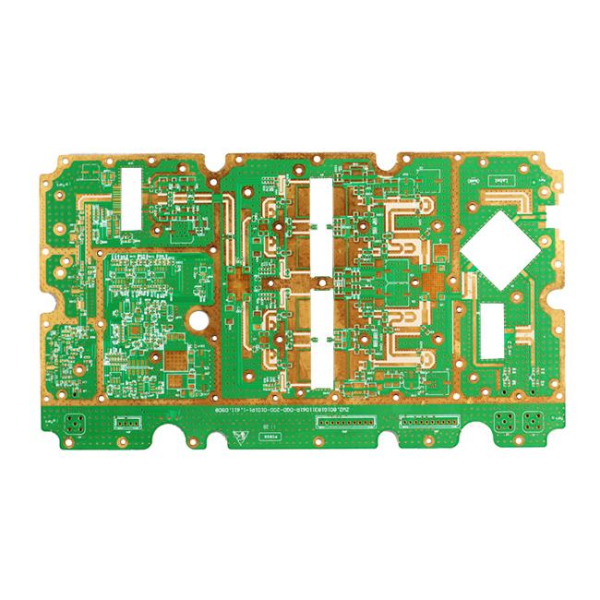
Complex devices with a large number of PCB assemblies and circuits benefit from the use of multilayer PCBs. Devices with multiple uses and advanced features require this complexity. As device miniaturization becomes an increasing trend, the use cases of multilayer PCBs will only increase. Many multilayer boards also have functions such as impedance control and electromagnetic interference shielding, which further improve the quality of the boards and equipment.
2. High power
Due to the high circuit density (such as HDI PCB), the circuit board is also more powerful. This means that they provide high operating capacity and speed, making them particularly suitable for advanced equipment.
3. Highly durable
As the number of layers increases, thicker boards are more durable. Therefore, it can withstand more severe conditions.
4. Size and volume
Small and light weight are additional features of multilayer boards. This makes them ideal for device miniaturization.
5. Single connection point
In terms of design simplicity and weight, the fact that they work with a single connection point is an additional advantage.
Therefore, in the current PCBA processing plant in Shenzhen, there is a phenomenon that the double panel and the single panel exist mutually, especially in the case of the combination of the main board and the sub board.