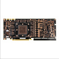
What factors should be considered while designing high speed PCB?
PCB layout is crucial
Efficient manufacturing of printed circuit boards (PCBs) used in high-speed circuits is critical to the end result. However, PCB layout design is usually not an active idea in this process. Advanced planning and compliance with important factors will greatly help provide a design that can achieve the required functions and successfully manufacture the PCB. These manufacturing design (DFM) and additional consideration of high-speed circuit requirements need to be addressed in the early stages of circuit board layout design, rather than an afterthought.
Poor layout can cause performance issues when the manufactured PCBs enter testing or production use. At this time, redesign or rework becomes more expensive and time-consuming because of evaluating circuit failures or performance issues and reconfiguring the prototype layout.
Precautions for PCB design
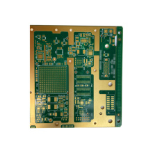
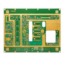
There are many factors that contribute to the success of PCB design in high-speed circuits:
Schematic documentation-detailed schematics form the basis of a good layout design. Problems often occur at manufacturing points related to the physical layout of the circuit board. By providing the expected flow of the circuit, a clear schematic diagram can save time to solve the problem. Include as much information as possible in the design schematic, including any details available, such as trace length, required component placement, circuit board enclosure information, etc.
Extra eyes-usually the circuit designer and engineer will not be the same person for the layout. In this case, it will add value to PCB layout technicians to consult initial designers to ensure that the layout meets the specific standards of the design. Collaborating at this stage of the design can save time and money in producing PCBs that operate as designed and meet expected results and performance levels.
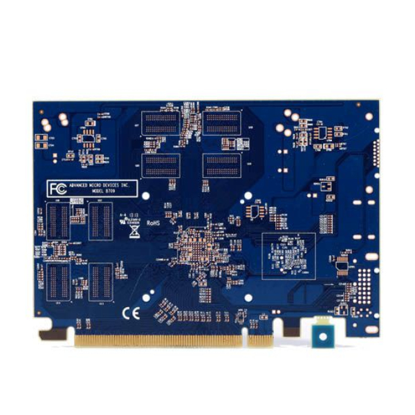
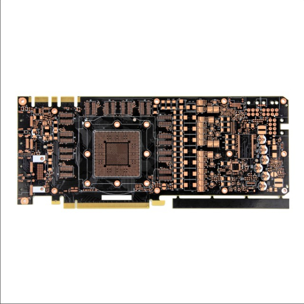
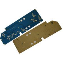
PCB assembly location-There are some major components that must clearly define the circuit board functions, such as key power supply locations and input/output points. The placement of other Electronic Components can also adversely affect the overall performance of the PCB, including placing a single circuit so that its physical proximity does not affect the function of another circuit.
Power supply-Power supply bypassing to minimize "noise" is particularly important for high-speed circuits. Common methods such as rail-to-ground or rail-to-rail can provide effective results.
Parasitics-High-speed circuits are usually negatively affected by unintended stray capacitance called parasitics. Understanding the potential source of this inductance and avoiding this potential instability or oscillation in the circuit is an important consideration in high-speed PCB design.
Other considerations regarding parasitic effects involve PCB design, including configuration ground plane utilization and packaging.
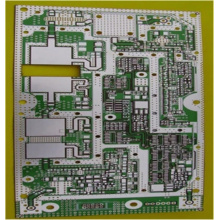
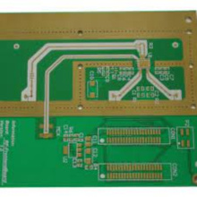
Wiring/shielding-The signals on the circuit board may interfere with each other, and for high-speed circuits, negative effects become more important. PCB designers must plan accordingly how the circuit board avoids such conflicts between signal paths through several techniques:
Maintain long parallel operation on the same circuit board
Reduce the appearance of long traces on adjacent circuit board layers
Keep the distance between signal traces as much as possible
If individual signal traces do require higher isolation, please route them on different layers if possible
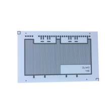
Materials-The manufacturing materials used in the board structure play an important role in reducing noise and signal crosstalk. Different materials have different dielectric constants, and a lower constant causes the signal to propagate at a higher speed.
Trace structure-The use of microstrip or stripline trace layout will also affect signal performance. The contributing values include trace width, thickness, and dielectric constant of the material in use. Each of these values affects the final Electronic Resistor and Capacitor of the trajectory, the performance of the related signal path, and the potential noise separation properties.
Successfully design high-speed PCB
Following best practices and guidelines for high-speed PCB design can minimize troubleshooting and rework. Record all design constraints reused by PCB design engineers and update them regularly. Develop a design consideration hierarchy that clearly explains the most critical considerations to the designer, making it second nature early in the development process.
The main goal is to produce work boards that are reliable and run as designed to achieve low cost pcb manufacturing.