Choose Shipping Method
Shipping Method Estimated Delivery Time Shipping Cost
Home > Electronic Components, Accessories & Telecommunications > PCB & PCBA > Multilayer PCB > Blind and Buried via PCB Multi...
  • 0 Piece/Pieces $ 0
  • ship to United States To Be Negotiated $ /
  • Lead time / days
    After payment is complete, your order will ship within
  • Shipping time / days
    Estimated Delivery Time is the time between your package shipped out of carriers’ warehouses and final destination delivery. Estimated delivery time does not include supplier manufacturing lead time, holidays and weekends.
Totals $ /
Blind and Buried via PCB Multilayer PCB assembly
  • Blind and Buried via PCB Multilayer PCB assembly
  • Blind and Buried via PCB Multilayer PCB assembly
  • Blind and Buried via PCB Multilayer PCB assembly
  • Blind and Buried via PCB Multilayer PCB assembly
  • Blind and Buried via PCB Multilayer PCB assembly
  • Blind and Buried via PCB Multilayer PCB assembly
  • Blind and Buried via PCB Multilayer PCB assembly
  • In Stock
  • Ready to Ship
  • Fast Dispatch

Blind and Buried via PCB Multilayer PCB assembly

  • $1.87
    ≥1
    Piece/Pieces
1 Piece/Pieces (Min. Order)
Quantity:

0 Piece,Product Price: US $ 0

  • Lead Time:/ days
  • Shipping time:/ days
  • Product Description
Overview
Product Attributes
Model No.:
Blind & Buried Vias
place of origin:
China
Number of layers:
4-Layer, 6-Layer, 8-Layer, 10-Layer, 12-Layer
Material:
Fr4/Cem-1/Cem-3/Fr1/Aluminum
Min. Hole Size:
0.25mm, 0.2mm
Min. Line Width:
3mil
Surface Finishing:
Osp
Board Thickness:
1.6mm
Copper Thickness:
0.5oz - 6.0oz
Layers:
1-28 L
Testing Service:
Aoi X-Ray Function Test
Packaging & Delivery
Selling Units:
Piece/Pieces
Single package size:
12cm*7cm*0.02cm
Single gross weight:
0.021kg
Package Type:
Vacuum packing
Picture Example:
Lead Time :
Quantity(Piece/Pieces) 1>1
Est. Time(days) 7To be negotiated

If you finish the payment today, your order will ship out within the delivery date.

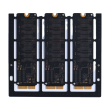
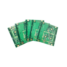
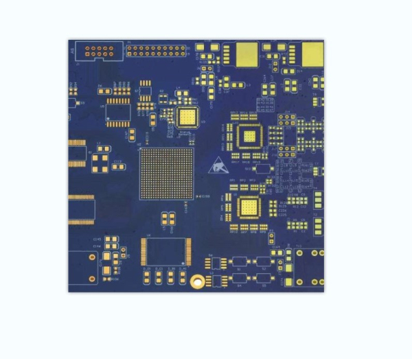
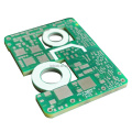
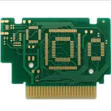
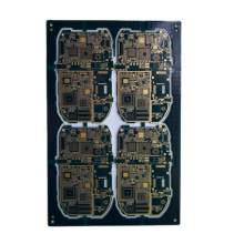
What is blind via in PCB?

BVH (buried/blind via hole) PCB. Also called buried PCB and blind via hole PCB. Referred to as BVH PCB.
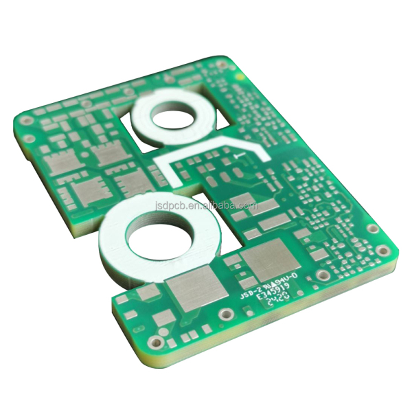
Blind Via Hole, which connects the outermost circuit of the PCB with the adjacent inner layer with electroplated holes. Because the opposite side cannot be seen, it is called "blind through". In order to increase the space utilization of the PCB circuit layer, a "blind via" process has emerged. This production method requires special attention to the depth of the drilling (Z axis) to be just right. This method often causes difficulties in electroplating in the hole, so it is almost used by no manufacturer; it is also possible to place the circuit layers that need to be connected in the individual circuit layers in advance. At that time, the holes should be drilled first, and then glued together, but a more precise positioning and alignment device is required.
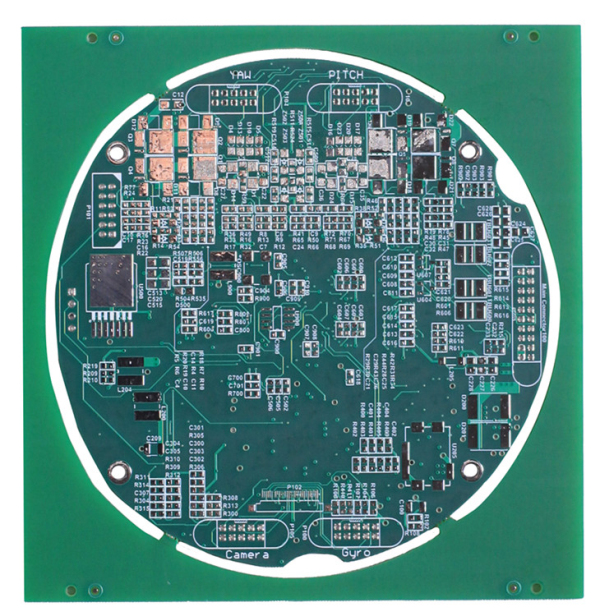
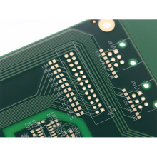
Blind vias are located on the top and bottom surfaces of custom pcb fabrication and have a certain depth. They are used to connect the surface line and the underlying inner line. The depth of the hole usually does not exceed a certain ratio (aperture).
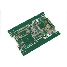
In the non-through via technology, the application of blind vias and buried vias can greatly reduce the size and quality of the PCB, reduce the number of layers, improve electromagnetic compatibility, increase the characteristics of electronic products, reduce costs, and also make the design work more Simple and fast. In traditional PCB design and processing, through holes can bring many problems. First, they occupy a large amount of effective space, and secondly, a large number of through holes are densely packed in one place, which also creates a huge obstacle to the inner layer wiring of the multilayer PCB. These through holes occupy the space required for the wiring, and they intensively pass through the power supply and the ground. The surface of the wire layer will also destroy the impedance characteristics of the power ground wire layer and make the power ground wire layer ineffective. And the conventional mechanical method of drilling will be 20 times the workload of non-through hole technology.
In PCB design, although the size of pads and vias have gradually decreased, if the thickness of the board layer is not proportionally reduced, the aspect ratio of the through hole will increase, and the increase of the aspect ratio of the through hole will reduce the reliability. With the maturity of advanced laser drilling technology and plasma dry etching technology, it is possible to apply non-penetrating small blind holes and small buried holes. If the diameter of these non-penetrating vias is 0.3mm, the parasitic parameters will be About 1/10 of the original conventional hole, which improves the reliability of the PCB.
Due to the non-through via technology, there are few large vias on the PCB, which can provide more space for routing. The remaining space can be used for large-area shielding purposes to improve EMI/RFI performance. At the same time, more remaining space can also be used for the inner layer to partially shield Electronic Components and key network cables, so that it has the best electrical performance. The use of non-through vias makes it easier to fan out the device pins, making it easy to route high-density pin devices (such as Surface-Mount (SMT) & BGA Assembly), shortening the wiring length, and meeting the timing requirements of high-speed circuits.

Blind And Buried Vias Eurocircuits JpgBlind Via And Buried Via JpgUnderstanding Blind And Buried Vias Jpg


Wholesale Blind And Buried Via Pcb Multilayer Pcb Assembly
You can browse a wide variety of products in every type to suit different parts of blind and buried via pcb multilayer pcb assembly. Browse traditional blind and buried via pcb multilayer pcb assembly, blind and buried via pcb and blind via and buried via pcb in different shapes, styles and sizes to suit the requirements and shop them at budget-friendly prices here. Our Bossgoomall offer great deals on these products to let you save a lot of money when you shop for decorative blind and buried via pcb multilayer pcb assembly, blind & buried vias pcb, blind and buried via pcb, blind via and buried via pcb, blind & buried vias pcb products at Bossgoomall. All these products are branded and known for effectiveness, vitality and long life. Change the mood of your place by picking from cost-effective and beautiful blind and buried via pcb multilayer pcb assembly products available at Bossgoomall!
You may like
Home > Electronic Components, Accessories & Telecommunications > PCB & PCBA > Multilayer PCB > Blind and Buried via PCB Multi...
Add To Cart Start Order
Sign in
Account
Password