0 Piece,Product Price: US $ 0
| Quantity(Piece/Pieces) | 1 | >1 |
| Est. Time(days) | 7 | To be negotiated |
If you finish the payment today, your order will ship out within the delivery date.
What is back drilling in PCB?
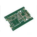
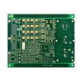
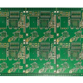
Via design in custom pcb fabrication
In high-speed PCB design, high frequency mixing pressure plate is often required, and vias are an important factor in multilayer PCB design. The via hole in the PCB is mainly composed of three parts: the hole, the pad area around the hole, and the POWER layer isolation area. Next, let's understand the problems and design requirements of vias in high-speed PCBs.
The impact of vias in high-speed PCBs:
In the high frequency mixing pressure plate multi-layer board, the Microwave radio frequency board signal is transmitted from one layer of interconnection line to another layer of interconnection line to realize the connection through vias. When the frequency is lower than 1 GHz, the vias can To achieve a good connection effect, its parasitic capacitance and inductance can be ignored. When the frequency is higher than 1 GHz, the parasitic effect of the via cannot be ignored on the signal integrity. At this time, the via appears as a discontinuous impedance breakpoint on the transmission path, which will cause signal reflection, delay, and attenuation. And other signal integrity issues. When the signal is transmitted to another layer through the via hole, the reference layer of the signal line also serves as the return path of the via hole signal, and the return current will flow between the reference layers through capacitive coupling and cause problems such as ground bounce.


Worry-free return
Product quality protection
Payment protection
Shipping protection
Copyright © 2024 BOSSGOOMALL. All rights reserved
版权所有 宁波全贸信息技术有限公司 浙ICP备12012821号-84