0 Piece,Product Price: US $ 0

| Quantity(Piece/Pieces) | 1 | >1 |
| Est. Time(days) | 7 | To be negotiated |
If you finish the payment today, your order will ship out within the delivery date.
What is HDI High Density Interconnect?
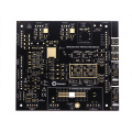
HDI High Quality PCB Products are printed circuit boards that have a higher wiring density per surface area than standard PCBs. HDI PCB uses some or all of the following functions to reduce the size of the PCB:
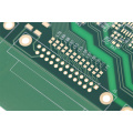
The line and pitch are less than or equal to 100 microns.
The through hole is less than or equal to 150 microns.
A hole less than or equal to 400 microns captures the pad.
The density of more than 20 pads per square centimeter.
The increased interconnect density allows for enhanced signal strength and improved reliability. In addition, due to the maximization of design efficiency and space, HDI-pcb makes it possible to manufacture smaller and more powerful electronic devices.
Why choose HDI PCB?
Why is there a separate PCB technology category called HDI? When the lines are less than 65 microns (2.559 mils), the ability to etch traces will be weakened, and traditional etching processes cannot be really used. For example, typical etching on standard boards allows very thick resists and standard imaging to be used on LDI machines, and there is basically enough space to accommodate any tolerances required to etch these spaces. In the microelectronics environment, there is generally no such room. These features are so tight that traditional etching processes cannot work.
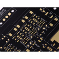
When PCB designers need higher density components, HDI technology is the best choice. So what is the difference between HDI and standard PCB? There are three main points:
1. In areas with higher PCB component density, use micro-holes instead of through-holes
2. Stacking alternatives to accommodate micro-holes
3. Arrange through holes to improve wiring
#1 Use micro-holes instead of vias, why use micro-hole HDI?
When higher-precision through-hole vias are required, HDI through-holes are used. The laser-drilled micro-holes can be used to a drilling depth of about 100µm. Since the microvias have short cylinders, they will not face problems due to the different CTE (Coefficient of Thermal Expansion) values of the substrate and copper. This is why micro vias are more suitable than through vias.
The best practice for designing high-efficiency HDI is to replace the most common through holes ("blind via holes, buried via holes, or through holes) with microvias. If there are no Electronic Components and traces on the most commonly used layers (for example: GND or PWR) (GND and PWR planes need to be solid and complete), move them to the top of the stack. This laminated structure can either eliminate the required vias, or use microvias instead of vias. Since the micro-holes do not pass through the pcb, this provides more space for other layers. Therefore, this approach can increase the routing density of the inner layer and reduce the number of signal layers.
#2 Layer stacking alternative, eliminating through-hole vias
Different stacking arrangements are used in the HDI structure to reduce the number of through holes and the number of inner layers. The ground and power planes are the most commonly used layers for vias. Designers can reduce the number of stacks by placing these layers on top of the stack (such as layer 2 and layer 3). The top and bottom layers are usually used for placement of Electronic Components.


Worry-free return
Product quality protection
Payment protection
Shipping protection
Copyright © 2024 BOSSGOOMALL. All rights reserved
版权所有 宁波全贸信息技术有限公司 浙ICP备12012821号-84