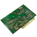
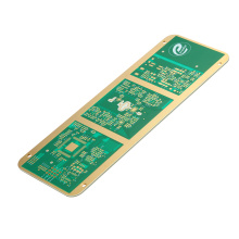
How do I choose a PCB material?
The life and performance of the PCB board depends on the choice of circuit board material. In order to select the correct circuit board material, it is important to check the materials that can be used for different circuit board categories. There are different characteristics and physical properties that help to choose a sheet. When evaluating PCB materials, it is necessary to ensure that the design requirements meet the required board performance.
When a large amount of current needs to be handled, the spacing and width of the circuit board are also important. The structural strength of the board is determined by the substrate and the laminate. The choice of materials for these two layers depends on the type of board.
The layers on the PCB and their significance
The PCB board consists of four layers, namely substrate, laminate, solder mask and screen printing. The substrate and laminate together define the basic electrical, mechanical and thermal circuit board properties
Substrate
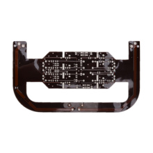
Glass fiber FR4 is the most common material used for PCB substrates. Here, FR stands for flame retardant. It is suitable due to its rigidity and thickness. For Custom Flexible PCB fabrication, use Kapton or equivalent plastics.
The thickness of the PCB board depends on its application or purpose. For example, most Sparkfun products have a thickness of 1.6mm, while Arduino Pro products have a thickness of 0.8mm. PCBs made of cheaper materials such as epoxy resin lack durability.
Substrates are found in low-cost consumer electronics products. These have low thermal stability, which causes them to easily lose lamination. When the soldering iron is fixed on the board for a long time, the substrate can also cause smoke, which makes them easy to identify.
The non-conductive layer of dielectric material is selected based on the dielectric constant.
The substrate must meet certain required properties, such as the glass transition temperature (Tg). Tg is the point at which heat causes the material to deform or soften. A variety of materials can be used for the substrate, such as aluminum or insulated metal substrate (IMS) FR-1 to FR-6, polytetrafluoroethylene (PTFE), CEM-1 to CEM-5, G-10 and G-11, RF-35, polyimide, alumina and flexible substrates such as Pyralux and Kapton.
"In general, IMSes can minimize thermal resistance and conduct heat more efficiently. These substrates are mechanically stronger than thick-film ceramic and direct-bonded copper structures commonly used in many applications."
Laminate
This provides properties such as coefficient of thermal expansion, tensile and shear strength, and Tg. Common dielectrics used for laminates are CEM-1 and CEM-3, FR-1, FR-4, polytetrafluoroethylene (Teflon), FR-2 to FR-6, CEM-1 to CEM-5 and G-10.
The copper foil is the next layer laminated to the board. For double-sided PCBs, copper is applied to both sides of the substrate. The thickness of copper varies according to the application. For example, compared to low-power applications, high-power applications have a larger thickness.
Solder mask
This is the layer on top of the copper foil. It can be used as an insulating material for copper traces to prevent accidental contact with other conductive metals. It helps to solder in the right place.
It is a protective layer that prevents external contamination and provides the required isolation between surface components such as pads, copper wires, and drilled holes.
Silk screen
Screen printing covers the solder mask and is used to add letters, numbers and symbols on the PCB to facilitate PCB assembly and better understand the circuit board through indicators.
PCB design technology
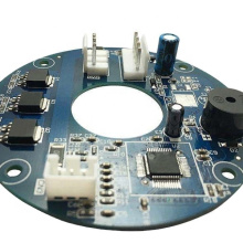
Each board has a unique purpose for a specific product. Therefore, it must be designed to perform this function in the allocated space. The designer uses a computer-aided design (CAD) system with special software to lay out the circuit patterns on the circuit board. Software that can be used for PCB design includes Allegro PCB Designer, Altium Designer and PCB Droid. The use of software ensures that the design does not contain errors, such as small or incorrect wiring or tiny holes.
"The two most common design techniques for PCB design are through-hole technology and surface mount technology (SMT). In the former, each component is pressed into a tiny hole in the substrate and soldered to connect to the back of the board. .
"In SMT chip processing, the L-shaped or J-shaped terminal of each component directly contacts the PCB.
"The components on the PCB are electrically connected to the circuit through these methods. Although SMT eliminates the time-consuming drilling process and space-consuming connection pads inherent in through-hole technology, you still need to be extra careful when placing Electronic Components."
Originality electronics IC has similar functions to PCB, the difference is that originality electronics IC contains more circuits and PCB components, these circuits and PCB components are grown on the surface of miniature silicon chips by electrochemical methods.
Safety precautions for toxic materials
The fumes in the solder may contain lead, which is toxic. Solder is used to make electrical connections on the PCB, so the soldering operation must be carried out in a closed environment. The smoke discharged into the atmosphere must be clean. One solution to replace wires and solder is to use water-soluble conductive molding plastics.
Precautions for choosing PCB materials for heat dissipation
The two factors that affect the PCB are power and heat. Therefore, it is important to determine each threshold. This can be done by evaluating the thermal conductivity of the PCB through the length of the material.
PCB materials with low thermal conductivity generate heat, which can be a huge disadvantage for heat-intensive applications.
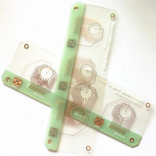
Choose PCB material
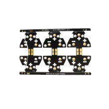
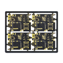
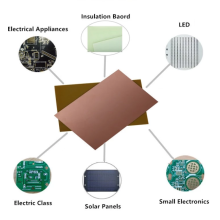
There are two types of PCBs, single-sided and double-sided, some of which are copper-clad, while others use aluminum in the military and aerospace, automotive and medical industries. For these specific areas, the materials used should have the best performance.
The reasons for choosing PCB materials are their light weight, good quality or the ability to withstand high power. Since the material level is related to the performance level, it is important to determine which functions need to be compared with each other when selecting PCB materials.
Most of the flexible board is composed of Kapton, which is a polyimide film with heat resistance, dimensional consistency and dielectric constant of only 3.6. Kapton has three Pyralux versions: FR, non-flame retardant (NFR) and glue-free, high performance (AP).
Quality is important for the construction of any type of circuit board for household electronic equipment or industrial equipment. Components such as PCBs should provide excellent performance over the expected lifetime. Electronic equipment, microwave ovens and other household appliances rely on PCB technology to keep them working.
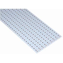
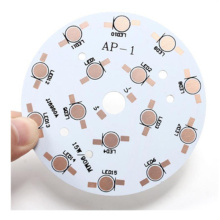
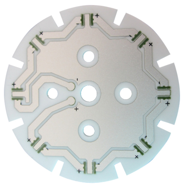
PCB for LED lighting
The LED PCB board heats up during operation. Therefore, the LED chip is mounted on an Aluminum base board made of metals such as aluminum, copper or alloy mixtures and coated with a highly reflective surface to achieve the best heat management and increase light output. This keeps the heat-generating components cool and improves their heat dissipation capacity. This can improve the performance and life of the LED.
Therefore, Metal Core PCB (MCPCB) was chosen for LED applications. It includes a thin layer of thermally conductive dielectric material, whose heat transfer efficiency is much higher than that of traditional rigid printed circuits. FR-4 material includes a layer of hot-dip aluminum, which can effectively dissipate heat. In view of the fact that MC-PCB materials are developed for higher power.