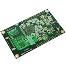
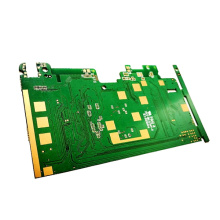
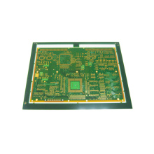
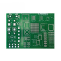
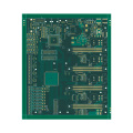
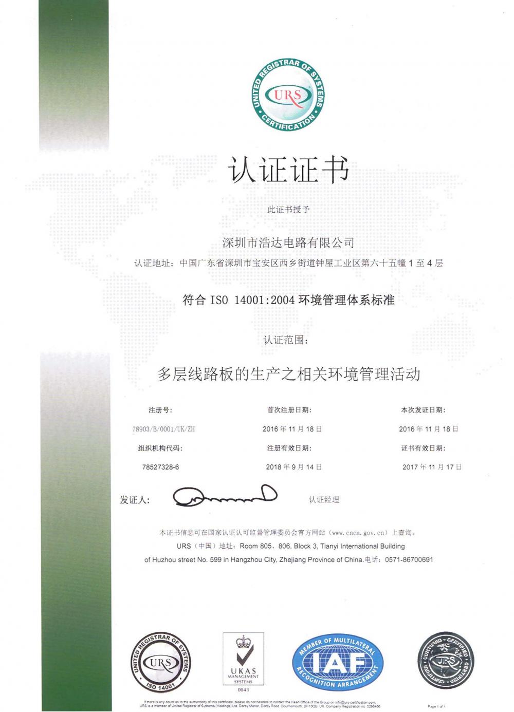
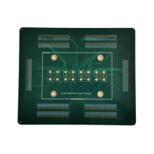
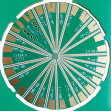
How to make a 6-layer PCB?
6-layer board refers to the printed circuit board PCB Printed Circuit Board is made of 6-layer glass fiber, usually SDRAM will use a 6-layer board, although it will increase the cost of the PCB but can avoid noise interference.
Six-layer board production steps and layout skills:
1. Editing of schematics
The 6-layer board can separate the analog ground from the digital ground because there can be two layers of ground in the PCB board. Regarding whether it is unified or separate, it involves the problem of the minimum return path of the signal in electromagnetic interference. After drawing the schematic diagram, don't forget to check the error and check the package manager to check the component package.
2. Create a new PCB file and set the layer structure
After the creation is completed, the schematic network table can be imported into the PCB file. The next thing to do is to set the layer structure (layer stack manager), add layer is to add an intermediate signal layer, and add plane is to add an internal power supply and an internal ground layer. The middle signal layer is the same as the top and bottom layers. Where signal lines are placed, the signal lines represent copper, and the places without signal lines are insulated. The internal power supply and the ground layer generate a layer of copper mold. The line used when dividing the internal electrical layer represents the corroded copper, that is to say, the dark red represents the corroded copper, and the other areas represent the copper mold. Another point is that the power plane and the main ground plane should be tightly coupled, and the interval is 5mil (prepreg).

Three, layout
The main principle of the layout is to do a good job of partitioning, that is, the partitioning of analog devices and digital devices, which can reduce interference, because the interference generated by digital signals is large, and the anti-interference is also strong, while the interference generated by analog signals is relatively small, but vulnerable Digital signal interference. Another point is to pay attention to the layout of components with different operating voltages, and devices with large voltage differences should be far apart. For some chip decoupling capacitors, the closer to the pin, the better. The other thing to pay attention to is that the pins of the same network are close, and the layout is beautiful.
In principle, there are 3 signal layers and 3 power layers, of which GND is two layers 2, 5, and the middle layers 3 and 4 are Power and middle signal layers. If there are few wires in the middle signal layer, copper can be applied to Power on the middle signal layer.
Fourth, the production of ground plane
Since the six-layer board has two ground layers, AGND and DGND are separated and located on the second and fourth layers respectively, so the operation of the ground network is relatively easy. Lead the ground network pins of the top and ground components with wires, and connect the via holes to the corresponding network (considering the production cost, try to use blind holes and buried holes as little as possible, and use pads instead of through holes). Minimize the use of pads during the connection process, because the pads will bring capacitance effects and increase interference.
Five, the production of the power plane
Since the multilayer board does not have only one working voltage value, the power layer generally needs to be divided. The specific steps of segmentation are as follows:
1. Highlight a certain voltage network, switch to the inner power layer, and use line to draw a closed graph. The closed area is the voltage network;
2. Lead the pins of the top layer and ground layer with wires and connect them to the inner power layer through the pads; 3. Draw the next power network. The line is the dividing line of the two networks, which is the part that is corroded. Attention should be paid to the inner electric layer: the separation distance of the area with large voltage difference should be wider; the unused copper mold can be placed on the plane to corrode its area during production; do not place the pad on the separation line to affect it and the inner Electrical contact.
Six, routing
Prepare the power layer and ground layer, and then you can route the signal lines. When routing important high-speed signal lines, it’s best to go in the inner signal layer. Another principle is that the signal should go on its own ground layer. For example, if the top layer is mostly analog signals, the second layer is best set to AGND . Since the layer structure has been set up in the front, this point needs to be considered when routing the signal line. In addition, when wiring, the layout of components needs to be adjusted appropriately to facilitate wiring. The wiring between the top layer and the ground layer is no different from that of a two-layer board.
For the inner signal layer, the routing method is wire-pad-inner electric layer. Prioritize layout and routing for DDR FPGA FPC cables, etc. Use 5mil (0.127mm) signal line trace width, power line use (16mil) 0.4mm line width, theoretically 10mil line can have an overcurrent of 1A.
1. For important signals, perform differential wiring, set wiring groups, and perform winding equal length processing.
2. For multi-pin function irrelevant pins such as FPGA, they can be set into groups to facilitate swap pin operation.
3. For BGA packaged devices, first carry out the wiring, lead out the outermost two layers of pins, and then carry out the wiring. For the pins on the inner layer that are difficult to lead out the wiring, you can lead them to other layers appropriately.
4. For DDR data lines, try to ensure that the data lines are in a cluster, and the clock lines are isolated from the data lines.
5. The connection between the two chips passes through two vias at most.
6. The schematic can be selected and then linked to the PCB. In this way, specific components can be effectively selected.
7. For those that cannot be led out next to the pins, they can be led to the outside and farther away.
8. For the GND and Power in the BGA, lead out the wires when wiring to avoid excessively dense wiring and unconnected GND and Power.
When the components are not dense and there is a certain empty area, it is best to lay the ground. The ground is also divided into AGND and DGND, so the local grounding operation should be carried out separately. It is generally necessary to fill teardrops.
8. DRC inspection
This step is very important. After the board is drawn, it must be carried out to check whether there are any violations of the rules that have not been found.