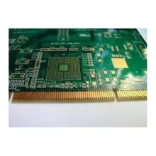
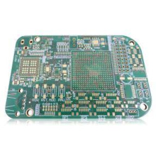
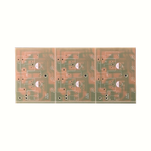
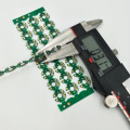
What is PCB testing?
The parts on the PCB are complex and diverse. Do these parts meet the specifications? Can all be welded? If it does not meet the process requirements, it cannot be manufactured rashly, otherwise it cannot be used. So, it is very important to test before PCBA Manufacturing. PCB test points are needed here. The so-called PCB test point is used to test whether the components on the circuit board meet the specifications and solderability.
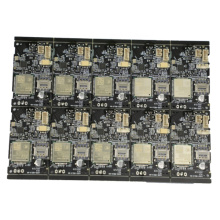
To measure PCB, ICT (In-Circuit-Test) is generally used, that is, an automated testing machine, which uses a bed of needles (Bed-Of-Nails) to contact all the parts on the board that need to be measured for testing. The speed of the testing machine is generally very fast, but when the probe touches the part or the solder foot, it may be crushed. In this way, the non-problem device becomes a problem instead.
To solve this problem, a "test point" appeared. A pair of small circular dots were drawn at both ends of the part. There is no mask on the part, so that the test probe can touch these small points. There is no need to directly touch the Electronic Components being measured, so there is no need to worry about the Electronic Components being damaged. After understanding the importance of test points, what are the process requirements when making test points?
1. The pads used for welding components cannot be used as test points, and special test pads must be designed separately. The pads are on the same side of the PCB, which is convenient for inspection and reduces the corresponding cost.
2. The test point is made of soft, easily penetrated, and non-oxidized metal to ensure reliable grounding and prolong the service life of the probe.
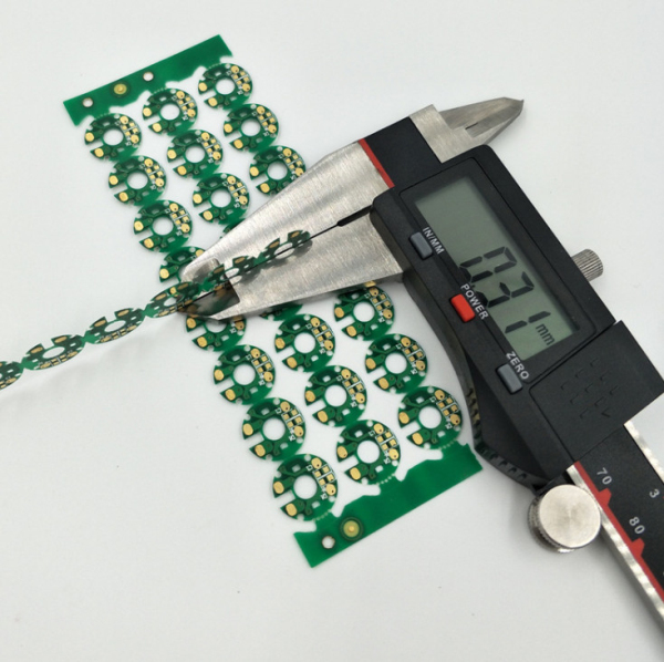
3. The distance between the test point and the edge of the PCB must be greater than 5mm; it must be placed 1mm away from the component to avoid collision between the probe and the component; it must be placed 3.2mm away from the ring of the positioning hole.
4. The diameter of the test point is not less than 0.4mm, and the distance between adjacent test points is preferably above 2.54mm, but not less than 1.27mm.
5. The test points should be evenly distributed on the PCB to reduce the pressure stress concentration of the probe; the power supply line on the PCB should be set with test breakpoints in different areas to facilitate power decoupling or fault point query.