Can PCBs be 3D printed?
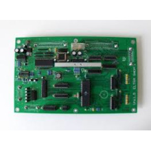
Nowadays, PCBs are still manufactured using traditional subtractive technology, usually the entire surface of the PCB is plated with copper, and areas that do not require copper are etched away from the board. This is like removing a lot of material from a piece of wood to get the desired shape and structure. There is a lot of waste in the process.
3D printing-additive manufacturing is just the opposite of subtracting materials. You can build materials as needed. Instead of first etching off the copper on the FR4 substrate, you start with a thin FR4 substrate, and then use conductive ink to add copper traces. This has brought material savings, 3D printing-additive manufacturing can reduce material costs and waste by up to 90%, and release the freedom of design and innovation. In the view of 3D Science Valley, it is this characteristic that makes 3D printed PCBs have the potential for paradigm shift.
Save materials and be more environmentally friendly
According to Autodesk-Autodesk, PCBs manufactured using additive manufacturing processes can provide:
-The higher the board density, the traces are distributed in a smaller area.
-Consistent trace definition and trace width can improve signal integrity.
-Thinner and more flexible circuits are ideal for wearable applications.
-Electrical and mechanical properties are more consistent.
-Electronic products with flexible/rigid circuits and varying trace thickness have better quality control.
There are two additive manufacturing solutions for electronic products-3D printing and 2D printing. In 3D printing, PCBs are printed layer by layer from scratch using a variety of conductive inks, gels, and substrates made at the level of nanoparticles.