0 Piece,Product Price: US $ 0
| Quantity(Piece/Pieces) | 1 | >1 |
| Est. Time(days) | 7 | To be negotiated |
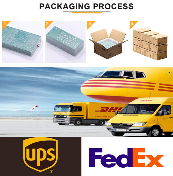
If you finish the payment today, your order will ship out within the delivery date.
What is the via filling in PCB?
Only when Via Filling is used on the PCB can the through holes be completely closed.
We can produce 2 types of channel filling:
Through hole filling resin
The through hole is filled with solder resist.
Through hole filling resin
Use the special machine ITC THP 30 to fill the special hole blocking resin TAIYO THP-100 DX1 thermosetting permanent hole filling material. The additional production steps required to fill the resin vias are performed before the 2-layer PCB production process. In the case of multiple layers, this is after pressing.
Overview of additional processes:
Only drill the vias that need to be blocked
Cleaning: Plasma and brushing
Black hole
Apply dry resist
Only through-hole imaging
Through Hole Plating (PTH)
Strip dry resist
If you need to brush your teeth
Baking: 150°C for 1 hour
Clogged by resin
Baking: 150°C for 1.5 hours
brush teeth
After these steps, the normal PCB production process begins or continues: drilling other PTH holes, and the normal outer layer production process.
Using IPC-4761 classified by the type of protection, this Via-filled process with resin always results in "Type VII-Fill and Cap" through holes.
Note: This type of through-hole filling resin is suitable for Via-in-Pad applications.
Through hole filling solder resist
Fill the through hole to be filled with solder resist ink as a hole filling substance. This Via Filling technology uses a drilled ALU board to push the ordinary solder mask ink in the through hole to the filler. This is a screen printing process. This is a step before the normal solder mask process.
important:
Filling is always done from the top of the board
The through hole filled with solder mask will always get a reverse solder mask pad, which is added by the tool size + 0.10mm. In other words, this type of Via Filling will always cover the solder mask on the top and bottom.
Using IPC-4761 classified by the protection type, this pass-through filling type and solder mask process always results in "VIb type-fill and cover" vias.
Note: This pass-through and solder mask type filler is not suitable for pass-through applications on pads.
Technical specifications
Through hole filling resin Through hole filling solder resist
ToolSize / EndSize (mm) min 0.20 / 0.10 0.20 / 0.10
max 0.60 / 0.50 0.60 / 0.50
Material thickness (mm) min 1.00 0.50
max 2.40 3.20
Outside StartCopper thickness (μm) min 18 NA
max NA NA
UL certification No Yes
IPC-4761 passes protection type VII-fill and cap VIb-fill and cover
Via-in-Pad application Yes No
Only PTH holes can be filled with through holes (PTH holes = holes with copper pads on the TOP and BOT sides).
BVH (buried/blind via hole) PCB only has through-holes and through-holes that can be filled with through-holes, so blind through-holes cannot be filled with through-holes.
The important parameters are the resin content, the aspect ratio of the pores and the thickness of the core involved. Complete filling cannot be guaranteed.
Avoid confusion between channel filling and channel blockage
IPC-4761 is classified by protection type to clearly define the difference between
Filling and plugging. In our manufacturing process, we only use Via Filling because it has a considerable advantage over Via plugging.


Worry-free return
Product quality protection
Payment protection
Shipping protection
Copyright © 2024 BOSSGOOMALL. All rights reserved
版权所有 宁波全贸信息技术有限公司 浙ICP备12012821号-84