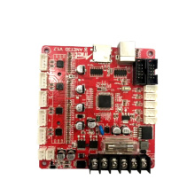
How to make ceramic PCB?
With the rapid development of power electronic circuits in the direction of integration and modularization, various new types of power Electronic Components continue to emerge, and the demand for power electronic devices continues to increase, resulting in an increasing demand for high-performance PCBs. At the same time, with the development of electronic, communication and other equipment in the direction of miniaturization, light weight, high reliability and high speed, especially to meet the needs of Surface-Mount (SMT) & BGA Assembly, the preparation of high-performance PCBs tends to be miniaturized and chip-type The development of high-quality, multi-layer, thin-film, and high-reliability directions requires PCBs with high stability, high thermal conductivity, high temperature resistance and low high-frequency loss.
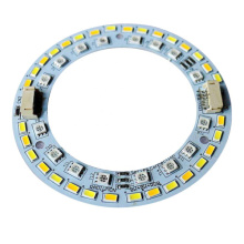
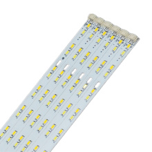
Ceramics are widely used in high-power power semiconductor modules, semiconductor refrigerators, and electronics due to their high insulation, high chemical stability, high thermal conductivity, and thermal expansion coefficient matching a variety of semiconductor device materials. In heaters and high-power power electronic circuits.

Because the surface structure of ceramic materials is different from the surface structure of metal materials, coupled with the special physical and chemical properties of the ceramic material itself, there are many characteristics and difficulties in preparing metal circuit patterns with high resolution, current density and overload power on the ceramic surface.
At present, there are thick film method, thin film method and dbc for metallization of ceramic surface.
The thick film method is mainly a high melting point metal method, including mo-mn method, silver-based brazing, screen printing, active metal powder sintering. It is made by coating paste on the ceramic surface and sintering in a heat treatment furnace. Part of the process needs to be carried out. Hydrogen reduction secondary treatment. This type of process has no restrictions on ceramic materials. The metal coating and ceramic have high bonding strength, but the disadvantages are very obvious. The processing temperature is above 900°C, high energy consumption, long production cycle, and low efficiency. It cannot be used to make multilayer and thin-film high-performance ceramic PCBs. It is mainly used as a seal between ceramics and metals, and has limited applications in the field of ceramic PCBs.
Thin film methods are mainly cvd/pvd, electroplating/electroless plating, and sputtering methods. This type of process can coat different types of ceramic surfaces with metal coatings, but the coating is thin, with many procedures, low efficiency, and high cost. This type of process As a supplementary process for patterning the metal layer on the ceramic surface, it has limited application in the field of ceramic pcb.
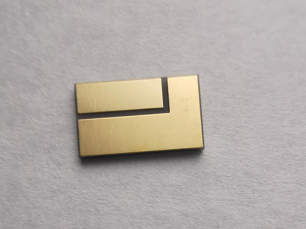
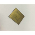
ceramics base copper-clad laminates is the abbreviation for direct bonded copper, which is a process of placing copper foil directly on alumina or aluminum nitride ceramics in a protective atmosphere, and keeping the temperature at 1065°C for 40-60 minutes. The eutectic reaction between the ceramics forms a transition layer, which is directly bonded to the ceramic surface. This process has fewer steps, can be used as a metal pattern or as a connecting metal, has high bonding strength, large current carrying, and strong solderability. It is the mainstream process for ceramic PCBs. Although this process has many advantages, it can only generate eutectic phases of complex oxides such as cu(alo2)2 and cu(alo2) on the surface of specific types of ceramics (aluminum nitride, alumina), thereby completing direct bonding on the ceramic surface. Combined with copper foil, the process is complicated and the cost is high.

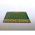
In summary, the ceramic substrate printed board, as a key process for preparing high-performance ceramic PCBs, has a difficulty in the metallization of the ceramic surface: either the processing temperature is too high, or the types of ceramic materials are limited. Therefore, there is a need for a high-performance ceramic pcb process with high resolution, current density, and overload power that has low processing temperature, high bonding strength, and no restrictions on the types of ceramic materials, to replace the current ceramic surface metallization medium-thick film method, The disadvantages of the thin film method and the dbc process.