Choose Shipping Method
Shipping Method Estimated Delivery Time Shipping Cost
Home > Electronic Components, Accessories & Telecommunications > PCB & PCBA > Other PCB & PCBA > One Stop Pcb Assemby Pcba Prot...
  • 0 Piece/Pieces $ 0
  • ship to United States To Be Negotiated $ /
  • Lead time / days
    After payment is complete, your order will ship within
  • Shipping time / days
    Estimated Delivery Time is the time between your package shipped out of carriers’ warehouses and final destination delivery. Estimated delivery time does not include supplier manufacturing lead time, holidays and weekends.
Totals $ /
One Stop Pcb Assemby Pcba Prototyping Service
  • One Stop Pcb Assemby Pcba Prototyping Service
  • One Stop Pcb Assemby Pcba Prototyping Service
  • One Stop Pcb Assemby Pcba Prototyping Service

One Stop Pcb Assemby Pcba Prototyping Service

  • $12
    ≥1
    Piece/Pieces
1 Piece/Pieces (Min. Order)
Quantity:

0 Piece,Product Price: US $ 0

  • Lead Time:/ days
  • Shipping time:/ days
  • Product Description
Overview
Product Attributes
Model No.:
PCB surface mount
place of origin:
China
price:
Fob Reference Price
Warranty period:
1 Year
PCB assembly process:
Circuit Board - Smd Dip - Assembly
smallest. Hole size:
0.2mm
Base material:
Fr4, High Tg Fr4, High Frequency, Alum, Fpc
Copper thickness:
1 Oz
minimum line/space:
0.075/0.075 Mm
Hole size:
Minimum Of 0.0078 "(0.2 Mm)
Other:
Aoi, X-Ray, Programming, Testing, Packaging, Plastic, Metal, The Coating
Resistance welding color:
Green, White, Black, Blue, Red...
Packaging & Delivery
Selling Units:
Piece/Pieces
Single package size:
9cm*8cm*5cm
Single gross weight:
0.19kg
Lead Time :
Quantity(Piece/Pieces) 1 ~ 5>5
Est. Time(days) 7To be negotiated

If you finish the payment today, your order will ship out within the delivery date.

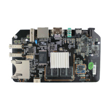
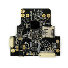
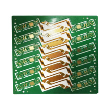
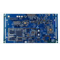
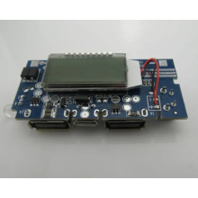
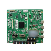
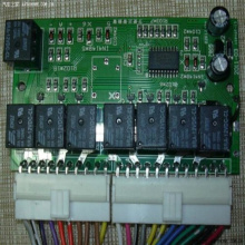
What is a surface mount PCB?

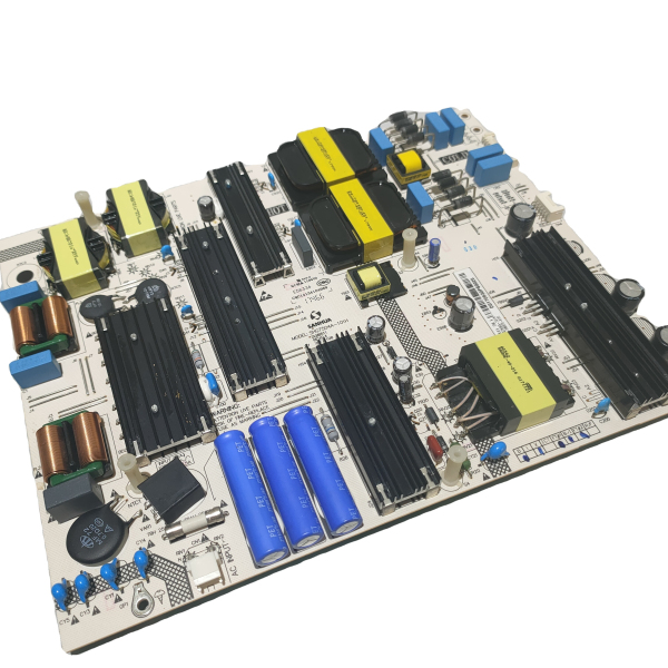
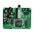
SMT patch refers to the abbreviation of a series of technological processes that are processed on the basis of PCB, which is part of the process of PCBA Manufacturing, and PCB is a printed circuit board. SMT is a surface mount technology (surface mount technology) is the most popular technology and process in the electronics assembly industry. It is a circuit assembly technology that mounts electronic components without leads or short leads on the surface of a printed circuit board or other substrates, and then solders them and PCB assembly by reflow soldering or Wave Solder for PCBA. . Under normal circumstances, the electronic products we use are designed by PCB plus various electronic components such as Electronic Resistor and Capacitor according to the designed circuit diagram, so all kinds of electrical appliances need a variety of different SMT chip processing techniques to process.

Pcb Design One Stop Service Jpg
SMT basic process components
1. Silk screen: Its function is to leak solder paste or patch glue onto the PCB pads to prepare for the soldering of components. The equipment used is a screen printing machine (screen printing machine), located at the forefront of the SMT production line.
2. Dispensing: It is to drip glue onto the fixed position of the PCB board, and its main function is to fix the components on the PCB board. The equipment used is a glue dispenser, located at the forefront of the SMT production line or behind the testing equipment.
Pcba One Stop Service Jpg
3. Mounting: Its function is to accurately mount the surface mount components to the fixed position of the PCB. The equipment used is a placement machine, located behind the screen printing machine in the SMT production line.
4. Curing: Its function is to melt the patch glue, so that the surface assembly components and the PCB board are firmly bonded together. The equipment used is a curing oven, located behind the placement machine in the SMT production line.
5. Reflow soldering: Its function is to melt the solder paste, so that the surface assembly components and the PCB board are firmly bonded together. The equipment used is a reflow oven, located behind the placement machine in the SMT production line.
6. Cleaning: Its function is to remove the solder residues such as flux that are harmful to the human body on the assembled PCB board. The equipment used is a washing machine, and the location may not be fixed, it may be online or offline.
Pcb Surface Mount Jpg
7. Inspection: Its function is to inspect the welding quality and assembly quality of the assembled PCBA board. The equipment used includes magnifying glass, microscope, online tester (ICT), flying probe tester, automatic optical inspection (AOI), X-RAY inspection system, functional tester, etc. The location can be configured in a suitable place on the production line according to the needs of the inspection.

Wholesale One Stop Pcb Assemby Pcba Prototyping Service
Are you still worrying about not finding the one stop pcb assemby pcba prototyping service? Come and find the one stop pcb assemby pcba prototyping service you want on Bossgoomall. If you want to know more about the products in one stop pcb assemby pcba prototyping service, Please click on the product details to view. we have the perfect after-sales service and technical support. Looking forward to your use of our products.
Home > Electronic Components, Accessories & Telecommunications > PCB & PCBA > Other PCB & PCBA > One Stop Pcb Assemby Pcba Prot...
Add To Cart Start Order
Sign in
Account
Password