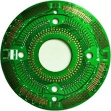
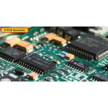
What is PCB manufacturing and assembly?
Regarding the PCB production process and process flow, the PCB production and PCBA production process are now integrated for analysis, and the form of articles combined with graphics and text is shared. If you have different opinions, you can also contact me to discuss and make progress together.
1. Cutting
Purpose: According to the requirements of the engineering data MI, on the large sheets that meet the requirements, cut into small pieces to produce panels. Small sheets that meet customer requirements.
Open material
Process: large sheet → cutting board according to MI requirements → curium board → beer fillet \ edging → ejecting board
2. Drilling
Purpose: According to the engineering data (customer data), drill the required hole diameter in the corresponding position on the sheet that meets the required size.
Process: stacked board pin → upper board → drilling → lower board → inspection \ repair
Three, sink copper
Purpose: Immersion copper is to deposit a thin layer of copper on the insulating hole wall by chemical method.
Process: rough grinding → hanging board → automatic copper sinking line → lower board → dip 1% dilute H2SO4 → thickened copper
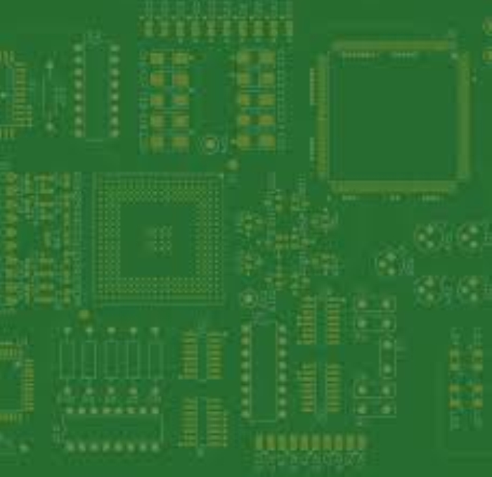
Four, graphics transfer
Purpose: Graphic transfer is to transfer the image on the production film to the board
Process: (blue oil process): grinding plate → printing the first side → drying → printing the second side → drying → exploding → developing shadow → inspection; (dry film process): hemp board → pressing film → standing → right Position→Exposure→Standing→Development→Check
Five, graphic plating
Purpose: Pattern electroplating is to electroplate a copper layer with the required thickness and a gold-nickel or tin layer with the required thickness on the bare copper skin or hole wall of the circuit pattern.
Process: upper board → degreasing → second washing with water → micro-etching → washing → pickling → copper plating → washing → pickling → tin plating → washing → lower board
Six, remove the film
Purpose: Use NaOH solution to remove the anti-electroplating coating film to expose the non-circuit copper layer.
Process: water film: insert rack → soak alkali → rinse → scrub → pass machine; dry film: release board → pass machine
Seven, etching
Purpose: Etching is to use a chemical reaction method to corrode the copper layer of non-circuit parts.
Eight, green oil
Purpose: Green oil is to transfer the graphics of the green film to the board to protect the circuit and prevent the tin on the circuit board when the Electronic Components are soldered.
Process: grinding plate→printing photosensitive green oil→curium plate→exposure→exposure; grinding plate→printing the first side→drying plate→printing the second side→drying plate.
Nine, characters
Purpose: Characters are provided as a mark for easy identification.
Process: After the green oil finishes → cool and stand → adjust the screen → print characters → rear curium.
Ten, gold-plated fingers
Purpose: Plating a nickel/gold layer with the required thickness on the finger of the plug to make it more hard and wear-resistant.
Process: upper plate → degreasing → washing twice → micro-etching → washing twice → pickling → copper plating → washing → nickel plating → washing → gold plating.
Ten, tin plate
Purpose: Tin spraying is to spray a layer of lead tin on the exposed copper surface that is not covered with solder mask to protect the copper surface from corrosion and oxidation and to ensure good soldering performance.
Process: micro-erosion → air drying → preheating → rosin coating → solder coating → hot air leveling → air cooling → washing and air drying.
11. Forming
Purpose: Organic gongs, beer boards, hand gongs, and hand-cutting methods are used to form the shapes required by customers through mold stamped printed wiring board or CNC gong machine.
Note: The accuracy of the data gong machine board and the beer board is higher. The hand gong is second, and the minimum hand-cutting board can only make some simple shapes.
12. Test
Purpose: To pass electronic 100% testing to detect defects that affect functionality such as open circuits and short circuits that are not easy to find visually.
Process: upper mold → release board → test → pass → FQC visual inspection → unqualified → repair → return test → OK → REJ → scrap
13. Final inspection
Purpose: Through 100% visual inspection of the board's appearance defects, and repair minor defects, pcb over 99.6% Satisfied rate, to avoid problems and defective boards from flowing out.
Specific work flow: incoming materials → check information → visual inspection → qualified → FQA spot check → qualified → packaging → unqualified → processing → inspection
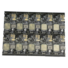
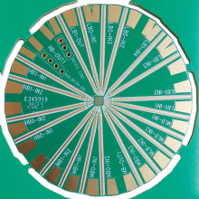
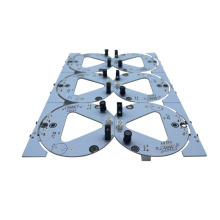
14. Slitting
PCBA boards are multi-connected boards, and need to use a PCB splitter for slitting. Different PCBA boards are cut by different PCB splitters.
Milling cutter dividing machine

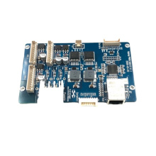
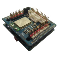
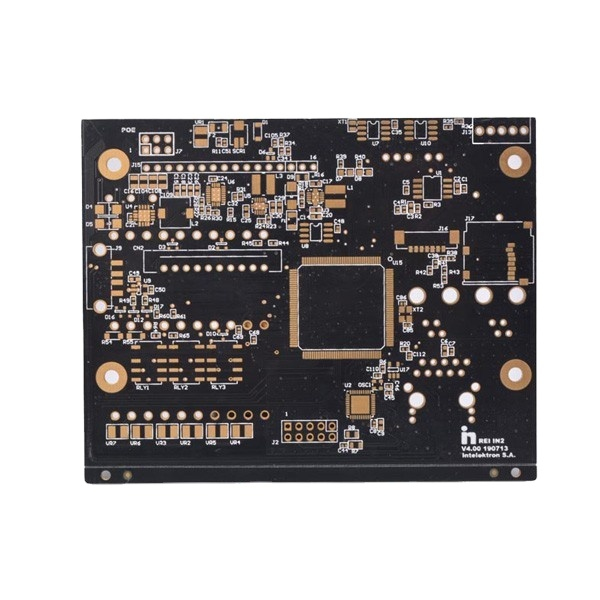
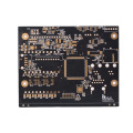
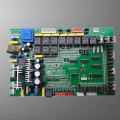
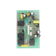
15. PCB assembly
After the PCBA board is cut by the PCBA splitter, PCB assembly is required.
The PCBA and manufacturing process involve many steps. If you want to obtain the best quality final product, PCBA Manufacturing, please perform the following steps:
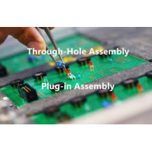
Step 1: Add solder paste: This is the initial stage of the assembly process. At this stage, solder paste is added to the electronic components pads wherever soldering is required. Put the solder paste on the pad and paste it in the correct position with the help of the soldering screen. This screen is made of PCB files and has holes.
Step 2: Place the component: After adding the solder paste to the component pad, it is time to place the component. The PCB passes through a machine that precisely places these components on the pads. The tension provided by the solder paste holds the components in place.
Step 3: Reflow oven: This step is used to permanently fix the components on the board. After placing the components on the board, the PCB passes through the reflow oven conveyor belt. The controlled heat of the oven melts the solder added in the first step, thereby permanently connecting the components.
Step 4: Wave Solder for PCBA: In this step, the PCB is passed through the molten solder wave. This will establish an electrical connection between the solder, PCB pads and component leads.
Step 5: Cleaning: Up to this step, all welding processes have been completed. During the soldering process, a large amount of flux residue will form around the solder joints. As the name suggests, this step involves cleaning flux residues. Clean the flux residue with deionized water and solvent. Through this step, PCB assembly is completed. The next steps will ensure that the assembly is completed correctly.
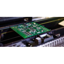
Step 6: Testing: At this stage, the PCB assembly is completed and inspections are started to test the position of the components. This can be performed in two ways:
Manual: This kind of inspection is usually carried out for smaller components, and the number of components does not exceed one hundred.
Auto: Perform this check to check whether there are bad joints, wrong components, wrongly placed components, etc.