0 Piece,Product Price: US $ 0
| Quantity(Piece/Pieces) | 1 | >1 |
| Est. Time(days) | 7 | To be negotiated |
If you finish the payment today, your order will ship out within the delivery date.
What is the purpose of vias?
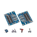
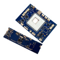
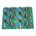
Via is one of the important components of multi-layer PCB, and the cost of drilling usually accounts for 30% to 40% of PCB manufacturing cost. To be more complicated, every hole on the PCB can be called a via. From the point of view of function, vias can be divided into two types: one is used for electrical connection between layers; the other is used for fixing or positioning of Electronic Components and Electronic connectors. As far as the process is concerned, these vias are generally divided into three categories, namely blind via PCB, buried via PCB and through via PCB. Blind holes are located on the outer surface of the top and bottom layers of the printed circuit board and have a certain depth. They are used to connect the surface circuit and the upper inner circuit. The depth of the hole usually does not exceed a certain ratio (aperture). Buried hole refers to the connection hole located in the inner layer of the printed circuit board, which does not extend to the surface of the circuit board. The above two types of holes are located in the inner layer of the circuit board, and the through hole forming process is used before lamination, and several inner layers can be stacked during the process of forming the via hole. The third type is called a through hole, which penetrates the entire circuit board and can be used to complete external interconnection or as a device positioning hole for Electronic Components. Because the through hole is easier to complete in the process and low cost pcb manufacturing, most of the printed circuit boards use it instead of the other two types of through holes. The via holes mentioned below, if not specifically clarified, are considered as via holes.


Worry-free return
Product quality protection
Payment protection
Shipping protection
Copyright © 2024 BOSSGOOMALL. All rights reserved
版权所有 宁波全贸信息技术有限公司 浙ICP备12012821号-84