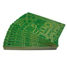
What is HDI in PCB?
HDI is the English abbreviation of High Density Interconnector, HDI PCB manufactured by High Density Interconnect (HDI). HDI High Quality PCB Products are structural elements formed by insulating materials and conductor wiring. When the printed circuit board is made into the final product, the Electronic Components will be installed on it. With the help of wire connection, it is possible to form an electronic signal connection and function. Therefore, the printed circuit board is a platform that provides component connection and is used to accept the substrate of the connected parts.
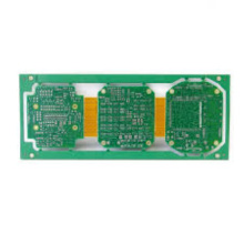
Under the premise that electronic products tend to be multi-functional and complex, the contact distance of origin electronics IC is reduced, and the speed of signal transmission is relatively increased. This is followed by an increase in the number of wiring and the locality of the length of the wiring between points. To shorten, these require the application of high-density circuit configuration and microvia technology to achieve the goal. Wiring and jumper are basically difficult to achieve for single and double panels, so the circuit board will be multi-layered, and because of the continuous increase of signal lines, more power layers and grounding layers are necessary means for design. All of these have made Multilayer Printed Circuit Board (Multilayer Printed Circuit Board) more common.
For the electrical requirements of high-speed signals, the circuit board must provide impedance control with alternating current characteristics, high-frequency transmission capabilities, and reduce unnecessary radiation (EMI). With the structure of Stripline and Microstrip, multi-layer design becomes a necessary design. In order to reduce the quality problems of signal transmission, insulating materials with low dielectric coefficient and low attenuation rate are used. To cope with the miniaturization and arraying of electronic components, the density of circuit boards is continuously increased to meet demand. The emergence of Surface-Mount (SMT) & BGA Assembly has promoted printed circuit boards to an unprecedented high-density state.
Holes with a diameter of less than 150um are called microvias in the industry. Circuits made using the geometric structure of this microvia technology can improve the efficiency of assembly, space utilization, etc., as well as the miniaturization of electronic products. Its necessity.
For circuit board products of this type of structure, the industry has had many different names to call such circuit boards. For example, European and American companies used to use sequential construction methods for their programs, so they called this type of product SBU (Sequence Build Up Process), which is generally translated as "Sequence Build Up Process." As for the Japanese industry, because the pore structure produced by this type of product is much smaller than that of the previous hole, the production technology of this type of product is called MVP (Micro Via Process), which is generally translated as "Micro Via Process." Some people call this type of circuit board BUM (Build Up Multilayer Board) because the traditional multi-layer board is called MLB (Multilayer Board), which is generally translated as "build-up multilayer board".
Based on the consideration of avoiding confusion, the IPC Circuit Board Association of the United States proposed to call this kind of product technology the general name of HDI PCB (High Density Intrerconnection) technology. If it is directly translated, it becomes a high-density interconnection. Technology. But this does not reflect the characteristics of the circuit board, so most circuit board manufacturers call this type of product HDI board or the full Chinese name "High Density Interconnection Technology". But because of the problem of the smoothness of spoken language, some people directly call this type of product "high-density circuit board" or HDI board.