Choose Shipping Method
Shipping Method Estimated Delivery Time Shipping Cost
Home > Electronic Components, Accessories & Telecommunications > PCB & PCBA > Single-Sided PCB > 6 Layer Laser Circuits
  • 0 Piece/Pieces $ 0
  • ship to United States To Be Negotiated $ /
  • Lead time / days
    After payment is complete, your order will ship within
  • Shipping time / days
    Estimated Delivery Time is the time between your package shipped out of carriers’ warehouses and final destination delivery. Estimated delivery time does not include supplier manufacturing lead time, holidays and weekends.
Totals $ /
6 Layer Laser Circuits
  • 6 Layer Laser Circuits
  • 6 Layer Laser Circuits
  • 6 Layer Laser Circuits
  • 6 Layer Laser Circuits
  • 6 Layer Laser Circuits
  • 6 Layer Laser Circuits
  • 6 Layer Laser Circuits
  • 6 Layer Laser Circuits
  • In Stock
  • Ready to Ship
  • Fast Dispatch

6 Layer Laser Circuits

  • $32
    ≥1
    Piece/Pieces
1 Piece/Pieces (Min. Order)
Quantity:

0 Piece,Product Price: US $ 0

  • Lead Time:/ days
  • Shipping time:/ days
  • Product Description
Overview
Product Attributes
Model No.:
6 Layer Laser Circuits
place of origin:
China
Base Material:
Fr4
Board Thickness:
1.6, 0.4-4.0mm
Copper Thickness:
1oz, 1/2oz 1oz 2oz 3oz
Min. Line Width:
0.075mm Or 3mil
Min. Line Spacing:
0.075mm Or 3mil, 0.1mm(4mil)
Min. Hole Size:
0.01'',0.25mm.Or 10 Mil
FOB Reference Price:
0.12
Get Latest Price:
Message Communication
Testing on products:
Testing Jig/Mold , X-Ray Inspection, Aoi Test, Functional Test
Surface treatment:
Hasl, Hasl Lead Free, Immersion Gold, Immersion Tin,
Packaging & Delivery
Selling Units:
Piece/Pieces
Single package size:
13cm*7cm*0.02cm
Single gross weight:
0.01kg
Package Type:
Vacuum packing
Picture Example:
Lead Time :
Quantity(Piece/Pieces) 1>1
Est. Time(days) 7To be negotiated

If you finish the payment today, your order will ship out within the delivery date.

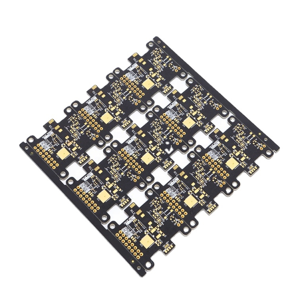
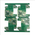
Can you laser etch PCB?

In custom pcb fabrication, direct laser imaging simplifies the pcb manufacturing process by at least 60%, while traditional film image transfer requires more than a dozen steps. So what are the methods for direct laser imaging in the PCB manufacturing process? The LDI equipment equipped with High Quality Prototype PCB Fabrication all over the world belongs to the LDI of UV light, which can be divided into three types according to its process:
1) Direct laser imaging of photoresist. This type refers to the direct laser imaging of the in-process plate coated with a special photoresist. To complete the conductive pattern on the board is based on the following three steps:
The first step: Facilitate the LDI sensitization of the special photoresist directly on the plate by the laser. Laser sensitization is controlled by cad graphic data or graphic data stored in the computer for laser scanning, and the photosensitivity of professional photoresist is much stronger than that of traditional photoresist (about 10 times). Laser scanning can achieve high PCB graphics transfer productivity.
The second step: chemical development. The special photoresist still uses the traditional weak alkaline sodium carbonate solution for development.
The third step: chemical etching. Since the dedicated photoresist is acid resistant (or the acid resistance is stronger than the alkali resistance), it is necessary to use an acidic copper chloride etching solution for etching.
2) PCB production adopts electroless tinning laser direct imaging.
The laser direct imaging (LDI) of electroless tin plating on the board is also called laser direct engraving in some literature. This type refers to the use of chemical methods to plate a very thin anti-corrosion layer tin on the system board, and then use laser etching to remove the tin layer that does not need to be etched and protected, and the thickness of the lower part (3μm~5μm) of copper The foil is then chemically etched. Since the tin layer is 0.5μm~1.0μm thick), it is alkali and acid resistant.
3) Direct imaging with the laser on the copper-clad board. This type refers to the direct imaging of the laser only on the copper-clad board. He does not need to apply any anti-corrosion protection layer to the board, but directly uses laser etching to remove the unnecessary copper foil, but in order to damage the thickness of the medium, often leave a 3μm~5μm thick copper foil, and then perform strict The thickness of the copper foil left by the controlled rapid chemical etching. Therefore, the copper thickness of the copper conductor pattern on the board will be thinner. This specific problem is analyzed in detail.
    In summary, we have learned about the type and method of laser direct imaging used in the PCB production process. The 6 Layer Laser Circuits process lies in excellence, continuous practice and optimization.

Microvias Blind Microvia Laser Drilling Jpg6 Layer Laser Drill Pcb Board JpgPth Drilling In Hdi Circuits JpgPrecision Cutting Of Printed Circuit Boards And Cover Layers JpgLaser Build Up Pcb Jpg6 Types Pcb Vias Jpg6 Layer Laser Circuits Jpg


Wholesale 6 Layer Laser Circuits
Are you still worrying about not finding the 6 layer laser circuits? Come and find the 6 layer laser circuits you want on Bossgoomall. If you want to know more about the products in 6 layer laser circuits, Please click on the product details to view. we have the perfect after-sales service and technical support. Looking forward to your use of our products.
Home > Electronic Components, Accessories & Telecommunications > PCB & PCBA > Single-Sided PCB > 6 Layer Laser Circuits
Add To Cart Start Order
Sign in
Account
Password