What are the 3 stages of reverse engineering?
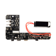
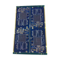
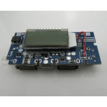
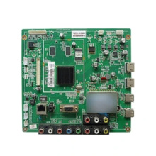
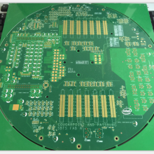
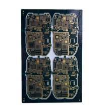
In PCBA reverse engineering, once you have an idea to build a model, you can use CAD (computer-aided design) models for custom pcb fabrication. To do this, you need the finished part to scan to build a CAD model, and then optimize the model. Some of the steps involved are described below.
Step 1: Retrieve data
The first step is to capture data from existing parts. For this, you can use various scanning devices according to the material and size of PCBA parts. Then, the scanner will generate 3D scan data output, such as a dense triangular mesh. This data will be used as a visual sketch, and you will need to do some operations to get the final CAD file.
Some PCB reverse engineering software used to capture data are mobile Faro arm, Faro laser scanner, etc.
Step 2: Perfect the model
After obtaining the detailed dimensions of the scanned documents, you can refine them into the final part. However, this process may vary depending on the reverse engineering software used. Improving the model involves the use of automation technology within the software and manual operations to assist the completion of the CAD model.
The point cloud or mesh form received from the scanner will now become a polygonal model. After that, you will clean, smooth and sculpt the resulting mesh to retain its desired shape and precision.
Step 3: Manufacturing
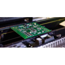
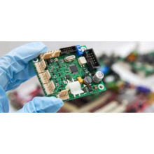
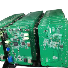
After the CAD model is completed, the part can be manufactured. Depending on the part size and its application, you may need to 3D print the CAD model to compare it with the original part before mass production.
In order to achieve High Quality Prototype PCB Fabrication.