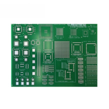
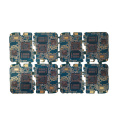
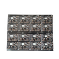
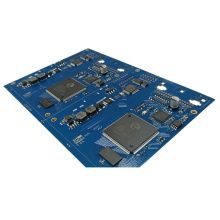
What is OSP finish in PCB?
High Quality Prototype PCB Fabrication must perform surface treatment on the PCB. Under the premise of ensuring the quality of PCB, to realize low cost pcb manufacturing, it is also necessary to carry out surface treatment on the PCB. How do we achieve pcb over 99.6% Satisfied rate? Principle: An organic film is formed on the copper surface of the circuit board, which firmly protects the surface of fresh copper, and can also prevent oxidation and pollution at high temperatures. OSP film thickness is generally controlled within 0.2-0.5 microns.
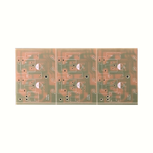
1. Process flow: degreasing → washing → micro-etching → washing → pickling → pure water washing → OSP → pure water washing → drying.
2. OSP material types: rosin (Rosin), active resin (ActiveResin) and azole (Azole). The OSP material used by www.pcbcoming.com is currently the most widely used azole OSP.
3. Features: good flat surface, no IMC is formed between the OSP film and the copper of the circuit board pad, allowing direct soldering of the solder and the circuit board copper during soldering (good wettability), low-temperature processing technology, low cost (low cost) For HASL), less energy use during processing, etc. It can be used on both low-tech circuit boards and high-density chip packaging substrates. Quick Turn PCB Proofing Youke Board Tips: ①The appearance inspection is difficult, and it is not suitable for multiple reflow soldering (usually three times); ②OSP film surface is easy to scratch ③High storage environment requirements; ④Short storage time
4. Storage method and time: 6 months in vacuum packaging (temperature 15-35℃, humidity RH≤60%).
5. Surface-Mount (SMT) & BGA Assembly site requirements: ① The OSP circuit board must be stored in low temperature and low humidity (temperature 15-35℃, humidity RH≤60%) and avoid exposure to acid gas-filled environment. After unpacking the OSP Start assembly within 48 hours; ②Single-side parts are recommended to be used within 48 hours, and it is recommended to store in a low-temperature cabinet instead of vacuum packaging; ③Surface-Mount (SMT) & BGA Assembly are recommended to complete DIP within 24 hours after the completion of both sides.